Definition and Purpose of Thermal Vias
What are Thermal Vias?
Thermal vias are specialized vias (vertical interconnect access) that are specifically designed to transfer heat from one layer of a PCB to another. Unlike regular vias, which are primarily used for electrical connectivity, thermal vias are optimized for heat dissipation. They provide a low-resistance thermal path that allows heat to flow efficiently from heat-generating components to heat sinks or other cooling solutions.
The Purpose of Thermal Vias
The primary purpose of thermal vias is to enhance the thermal management of PCBs. Electronic components, such as high-power processors, FPGAs, and power regulators, generate significant amounts of heat during operation. If this heat is not effectively dissipated, it can lead to several problems:
- Reduced performance: Excessive heat can cause components to operate outside their optimal temperature range, leading to reduced performance and efficiency.
- Decreased reliability: High temperatures can accelerate the aging process of electronic components, reducing their lifespan and increasing the risk of failure.
- Thermal stress: Temperature gradients across the PCB can cause thermal stress, potentially leading to warping, cracking, or delamination of the board.
By incorporating thermal vias into the PCB Design, designers can provide an efficient pathway for heat to dissipate from critical components to heat sinks or other cooling solutions. This helps maintain optimal operating temperatures, improves reliability, and prevents thermal-related issues.
Types of Thermal Vias
There are several types of thermal vias used in PCB design, each with its own characteristics and applications. Let’s explore the most common types:
1. Filled Thermal Vias
Filled thermal vias are vias that are completely filled with a thermally conductive material, such as copper or a specialized thermal compound. The filling process eliminates air gaps within the via, providing a solid thermal path for heat transfer. Filled thermal vias offer several advantages:
- Enhanced thermal conductivity: The solid filling material provides a direct and efficient thermal path, reducing Thermal Resistance and improving heat dissipation.
- Improved mechanical strength: Filled vias add structural integrity to the PCB, reducing the risk of via cracking or delamination.
- Increased reliability: By eliminating air gaps, filled vias minimize the risk of moisture ingress and improve the overall reliability of the PCB.
However, filled thermal vias also have some limitations. The filling process adds complexity and cost to the manufacturing process. Additionally, filled vias may have limited electrical connectivity, as the filling material may not be electrically conductive.
2. Plated Thermal Vias
Plated thermal vias are vias that are plated with a thermally conductive material, typically copper, along the inner walls of the via. The plating process creates a thin layer of conductive material that facilitates heat transfer. Plated thermal vias offer several benefits:
- Improved thermal conductivity: The plated layer enhances heat transfer compared to non-plated vias, providing a more efficient thermal path.
- Electrical connectivity: Unlike filled vias, plated vias maintain electrical connectivity, allowing them to serve both thermal and electrical purposes.
- Cost-effective: Plated thermal vias are generally less expensive to manufacture compared to filled vias, as the plating process is more straightforward.
However, plated thermal vias may have limitations in terms of thermal performance compared to filled vias, as the plating layer is relatively thin and may not provide the same level of thermal conductivity.
3. Capped Thermal Vias
Capped thermal vias are a combination of filled and plated vias. They consist of a plated via that is partially filled with a thermally conductive material, leaving a small air gap at the top. The air gap is then capped with a conductive material, such as copper or solder. Capped thermal vias offer several advantages:
- Enhanced thermal performance: The combination of plating and partial filling provides excellent thermal conductivity, while the capped air gap allows for some flexibility and stress relief.
- Improved reliability: The capped design prevents moisture ingress and provides a more robust mechanical structure compared to non-capped vias.
- Electrical connectivity: Like plated vias, capped vias maintain electrical connectivity, allowing them to serve both thermal and electrical functions.
Capped thermal vias strike a balance between the thermal performance of filled vias and the cost-effectiveness of plated vias. However, the capping process adds an additional manufacturing step, which may increase the overall cost.

Design Considerations for Thermal Vias
When incorporating thermal vias into PCB design, several key considerations need to be taken into account to ensure optimal performance and manufacturability. Let’s explore these design considerations in detail:
1. Via Size and Pitch
The size and pitch of thermal vias play a crucial role in their thermal performance and manufacturability. Via size refers to the diameter of the via, while pitch refers to the distance between the centers of adjacent vias.
Larger via sizes generally provide better thermal conductivity, as they offer a greater cross-sectional area for heat transfer. However, larger vias also consume more board space and may impact routing density. Designers need to strike a balance between thermal performance and board real estate.
The pitch of thermal vias also affects their thermal performance and manufacturability. A smaller pitch allows for more vias to be placed in a given area, enhancing heat dissipation. However, a pitch that is too small may pose manufacturing challenges and increase the risk of via-to-via shorting.
Designers should consider the capabilities of their PCB Fabrication partner and adhere to their recommended via size and pitch guidelines to ensure manufacturability and reliability.
2. Via Placement and Pattern
The placement and pattern of thermal vias are critical factors in optimizing heat dissipation. Thermal vias should be strategically placed in close proximity to heat-generating components to provide an efficient thermal path.
There are several common via placement patterns used in PCB design:
- Grid pattern: Thermal vias are arranged in a regular grid pattern, providing uniform heat dissipation across the component footprint.
- Staggered pattern: Vias are arranged in an alternating pattern, which can help increase the number of vias in a given area while maintaining manufacturability.
- Concentric pattern: Vias are placed in concentric circles around the heat source, providing a radial heat dissipation path.
The choice of via placement pattern depends on factors such as the component footprint, available board space, and thermal requirements. Designers should also consider the thermal resistance of the PCB material and the thermal interface between the component and the PCB when determining via placement.
3. Thermal Interface Materials
Thermal interface materials (TIMs) play a crucial role in enhancing the thermal transfer between components and thermal vias. TIMs are used to fill the gaps and irregularities between the component package and the PCB surface, improving thermal contact and reducing thermal resistance.
Common types of TIMs include:
- Thermal greases: These are thick, paste-like materials that are applied between the component and the PCB. They conform to surface irregularities and provide good thermal conductivity.
- Thermal Pads: These are pre-cut, thermally conductive pads that are placed between the component and the PCB. They offer ease of application and consistent thickness.
- Phase-change materials: These materials change from a solid to a liquid state at a specific temperature, allowing them to conform to surface irregularities and improve thermal contact.
The selection of the appropriate TIM depends on factors such as the component package, thermal requirements, and manufacturing process. Designers should consider the thermal conductivity, thickness, and ease of application when choosing a TIM.
4. PCB Stack-up and Layer Configuration
The PCB stack-up and layer configuration play a significant role in the thermal management of the board. The number of layers, their arrangement, and the materials used can impact the thermal performance of the PCB.
When designing a PCB stack-up for thermal management, consider the following:
- Thermal conductivity of the PCB materials: Choose materials with high thermal conductivity, such as copper or specialized thermal substrates, to enhance heat dissipation.
- Thermal vias in ground and power planes: Placing thermal vias in the ground and power planes can help spread heat across the PCB and improve overall thermal performance.
- Thermal via spacing and density: Optimize the spacing and density of thermal vias to ensure efficient heat transfer while maintaining signal integrity and manufacturability.
Designers should work closely with their PCB fabrication partner to determine the optimal stack-up and layer configuration for their specific application and thermal requirements.

Best Practices for Implementing Thermal Vias
To ensure the effective implementation of thermal vias in PCB design, consider the following best practices:
1. Collaborate with PCB Fabrication Partners
Engage with your PCB fabrication partner early in the design process to discuss your thermal management requirements and design constraints. They can provide valuable insights into via sizes, pitches, and manufacturing capabilities specific to your project.
2. Conduct Thermal Simulations
Utilize thermal simulation tools to analyze the thermal performance of your PCB design. These simulations can help identify hot spots, optimize via placement and density, and validate the effectiveness of your thermal management strategy.
3. Consider Via Reliability
When designing thermal vias, consider the reliability aspects, such as via cracking and delamination. Ensure that the via design and placement adhere to industry standards and guidelines to minimize the risk of reliability issues.
4. Document and Communicate Design Intent
Clearly document and communicate your thermal via design intent to all stakeholders, including the PCB fabrication team, assembly team, and test engineers. Provide detailed specifications, drawings, and guidelines to ensure consistent implementation and verification of the thermal via design.
5. Test and Validate Thermal Performance
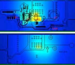
Conduct thorough testing and validation of the thermal performance of your PCB design. Use thermal imaging cameras, thermocouples, or other temperature measurement techniques to verify that the thermal vias are effectively dissipating heat and maintaining the desired operating temperatures.
By following these best practices, designers can optimize the implementation of thermal vias and ensure the reliable and efficient thermal management of their PCB designs.

Frequently Asked Questions (FAQ)
-
Q: What is the difference between thermal vias and regular vias?
A: Thermal vias are specifically designed for heat dissipation, while regular vias are primarily used for electrical connectivity. Thermal vias are typically larger in size and may be filled or plated with thermally conductive materials to enhance heat transfer. -
Q: How do I determine the appropriate size and pitch of thermal vias?
A: The size and pitch of thermal vias depend on various factors, including the thermal requirements, available board space, and manufacturing capabilities. Consult with your PCB fabrication partner to determine the recommended via size and pitch for your specific application. -
Q: Can thermal vias be used for electrical connectivity as well?
A: Yes, thermal vias can serve both thermal and electrical purposes, depending on their design. Plated and capped thermal vias maintain electrical connectivity, while filled vias may have limited electrical functionality. -
Q: What are the advantages of using filled thermal vias?
A: Filled thermal vias offer enhanced thermal conductivity, improved mechanical strength, and increased reliability compared to non-filled vias. The solid filling material provides a direct and efficient thermal path for heat dissipation. -
Q: How do I select the appropriate thermal interface material (TIM) for my PCB design?
A: The selection of the appropriate TIM depends on factors such as the component package, thermal requirements, and manufacturing process. Consider the thermal conductivity, thickness, and ease of application when choosing a TIM. Consult with your PCB fabrication partner or TIM supplier for recommendations specific to your application.
Conclusion
Thermal vias are a critical component in the thermal management of PCBs. By providing an efficient pathway for heat dissipation, they help maintain optimal operating temperatures, improve reliability, and prevent thermal-related issues in electronic devices.
Understanding the types of thermal vias, design considerations, and best practices for implementation is essential for designers to effectively incorporate thermal vias into their PCB designs. Collaborating with PCB fabrication partners, conducting thermal simulations, and thorough testing and validation are key steps in ensuring the successful implementation of thermal vias.
As electronic devices continue to push the boundaries of performance and power density, the role of thermal vias in PCB design becomes increasingly important. By leveraging the benefits of thermal vias and following best practices, designers can create robust and reliable PCBs that can withstand the thermal challenges of modern electronics.
| Thermal Via Type | Description | Advantages | Limitations |
|---|---|---|---|
| Filled | Completely filled with thermally conductive material | Enhanced thermal conductivity, improved mechanical strength, increased reliability | Added complexity and cost, limited electrical connectivity |
| Plated | Plated with thermally conductive material along the inner walls | Improved thermal conductivity, electrical connectivity, cost-effective | Limited thermal performance compared to filled vias |
| Capped | Partially filled with thermally conductive material and capped | Enhanced thermal performance, improved reliability, electrical connectivity | Additional manufacturing step, increased cost compared to plated vias |
| Design Consideration | Description |
|---|---|
| Via Size and Pitch | Balance thermal performance, board space, and manufacturability |
| Via Placement and Pattern | Strategic placement near heat-generating components, consider pattern options |
| Thermal Interface Materials | Select appropriate TIM based on component package, thermal requirements, and manufacturability |
| PCB Stack-up and Layer Configuration | Choose materials with high thermal conductivity, optimize via spacing and density |
By considering these design aspects and following best practices, designers can effectively implement thermal vias to achieve optimal thermal management in their PCB designs.


Leave a Reply