Understanding the PCB Silkscreen
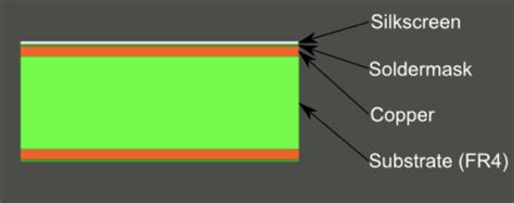
The PCB silkscreen, also known as the legend or nomenclature, is a layer of text and symbols printed on the surface of a PCB. It is typically white in color and is applied using a silkscreen printing process, hence its name.
Purpose of the PCB Silkscreen
The primary purpose of the silkscreen is to provide clear and concise information about the components, connectors, and other features on the PCB. This information is crucial for several reasons:
-
Assembly: The silkscreen helps guide the placement of components during the assembly process, ensuring that each component is installed in the correct location and orientation.
-
Debugging: When troubleshooting a PCB, the silkscreen can help identify specific components, test points, and other features, making it easier to diagnose and fix issues.
-
Maintenance: The silkscreen provides a quick reference for technicians performing maintenance or repairs on the PCB, allowing them to easily identify and replace components as needed.
Common Silkscreen Elements
The silkscreen typically includes the following elements:
-
Component designators: These are the unique identifiers for each component on the PCB, such as R1 for a resistor or C2 for a capacitor.
-
Polarity indicators: Symbols or text indicating the polarity of components like electrolytic capacitors, diodes, and LEDs.
-
Connector pinouts: Labels for the pins on connectors, helping to ensure proper wiring and connection.
-
Test points: Labeled test points for probing signals or voltages during debugging or testing.
-
Company logos and product information: Branding elements and product-specific information, such as model numbers or serial numbers.
The Silkscreen Printing Process
The silkscreen is applied to the PCB using a specialized printing process that involves the following steps:
-
Artwork creation: The silkscreen artwork is created using CAD software, ensuring that all text and symbols are properly sized and positioned.
-
Screen preparation: A fine mesh screen is coated with a light-sensitive emulsion and exposed to UV light through the artwork, hardening the emulsion in the areas where the artwork is transparent.
-
Ink application: The screen is placed over the PCB, and ink is forced through the open areas of the screen onto the PCB surface using a squeegee.
-
Curing: The printed PCB is then cured, typically using heat, to ensure that the ink adheres properly to the surface and becomes resistant to abrasion and chemicals.
Silkscreen Ink
The ink used for the silkscreen is a specialized epoxy-based ink that is designed to adhere well to the PCB surface and withstand the harsh conditions of the manufacturing process and the end-use environment. The ink is typically white in color to provide high contrast against the green solder mask of the PCB, making it easy to read.
Silkscreen Resolution and Limitations
The resolution of the silkscreen is limited by the mesh size of the screen used in the printing process. Typically, the minimum line width and spacing for the silkscreen is around 0.15mm (6 mils). Text should be at least 1mm (40 mils) in height to ensure legibility.
It’s essential to keep these limitations in mind when designing the silkscreen artwork to ensure that all elements are clear and easy to read.

Silkscreen Design Best Practices
To create an effective and informative silkscreen, consider the following best practices:
-
Keep it simple: Use clear, concise text and symbols to convey information, avoiding clutter and unnecessary elements.
-
Use standard designators: Follow industry-standard designator formats, such as R for resistors, C for capacitors, and U for integrated circuits.
-
Maintain clearance: Ensure that there is sufficient clearance between the silkscreen elements and the components, pads, and traces on the PCB to avoid interfering with soldering or assembly.
-
Orient text appropriately: Position text and symbols so that they are easily readable when the PCB is installed in its final orientation.
-
Consider multilingual requirements: If the PCB will be used in multiple regions or by users who speak different languages, consider including multilingual text or universally understood symbols.

Frequently Asked Questions (FAQ)
1. Can the silkscreen be applied to both sides of the PCB?
Yes, the silkscreen can be applied to both the top and bottom surfaces of the PCB, depending on the design requirements and the location of components and features.
2. Is the silkscreen required on every PCB?
While the silkscreen is not strictly required for the functional operation of the PCB, it is highly recommended for most applications to aid in assembly, debugging, and maintenance.
3. Can the silkscreen be customized with different colors or artwork?
In most cases, the silkscreen is limited to a single color (typically white) due to the nature of the printing process. However, some manufacturers may offer custom silkscreen options for specific applications or higher-volume orders.
4. How durable is the silkscreen?
The epoxy-based ink used for the silkscreen is designed to be durable and resistant to abrasion, chemicals, and environmental factors. However, excessive abrasion or exposure to harsh chemicals can degrade the silkscreen over time.
5. Can the silkscreen be modified or updated after the PCB has been manufactured?
Modifying the silkscreen after the PCB has been manufactured is not typically possible, as it would require repeating the entire silkscreen printing process. Any necessary changes should be made to the artwork before the PCB is manufactured.

Conclusion
The PCB silkscreen is a critical component that provides essential information for assembly, debugging, and maintenance. By understanding the purpose, elements, and best practices for designing the silkscreen, you can create PCBs that are easier to work with and maintain throughout their lifecycle.
| Silkscreen Element | Purpose |
|---|---|
| Component designators | Unique identifiers for each component on the PCB |
| Polarity indicators | Symbols or text indicating the polarity of components |
| Connector pinouts | Labels for the pins on connectors |
| Test points | Labeled test points for probing signals or voltages |
| Company logos and product information | Branding elements and product-specific information |
As PCB designs continue to evolve and become more complex, the importance of a clear and informative silkscreen will only continue to grow. By staying up-to-date with best practices and working closely with your PCB manufacturer, you can ensure that your PCBs are equipped with silkscreens that effectively support your assembly, debugging, and maintenance needs.


Leave a Reply