Understanding PCB trace width
PCB trace width is a crucial aspect of printed circuit board (PCB) design that significantly impacts the overall performance, reliability, and manufacturability of the board. The width of a PCB trace refers to the physical dimension of the conductive copper pathways that carry electrical signals between components on the board. Properly designing PCB trace widths is essential to ensure that the board functions as intended and meets the required specifications.
Factors Affecting PCB Trace Width
Several factors influence the determination of appropriate PCB trace widths:
- Current carrying capacity
- Signal integrity
- Manufacturing constraints
- PCB layer stack-up
- Cost considerations
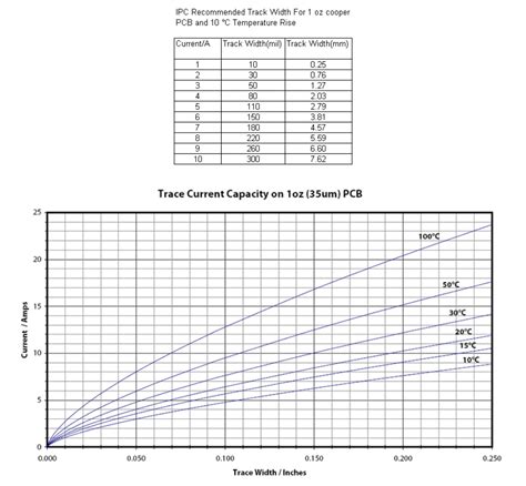
Current Carrying Capacity
One of the primary functions of PCB traces is to carry electrical current between components. The width of a trace directly affects its current carrying capacity, also known as ampacity. Wider traces can handle higher currents without overheating or suffering from excessive voltage drop. The current carrying capacity of a trace is determined by several factors, including:
- Copper thickness (oz/ft²)
- Trace length
- Ambient temperature
- Maximum allowable temperature rise
The following table provides a general guideline for the current carrying capacity of PCB traces based on their width and copper thickness:
| Trace Width (mm) | 1 oz/ft² (A) | 2 oz/ft² (A) |
|---|---|---|
| 0.25 | 0.5 | 0.7 |
| 0.50 | 1.0 | 1.4 |
| 0.75 | 1.5 | 2.1 |
| 1.00 | 2.0 | 2.8 |
| 1.50 | 3.0 | 4.2 |
| 2.00 | 4.0 | 5.6 |
Note: These values are approximate and may vary based on specific design requirements and environmental conditions.
Signal Integrity
PCB trace width also plays a significant role in maintaining signal integrity. High-speed digital signals and sensitive analog signals can be adversely affected by factors such as impedance mismatch, crosstalk, and electromagnetic interference (EMI). Properly designing trace widths can help mitigate these issues and ensure reliable signal transmission.
Controlled Impedance
In high-speed digital designs, it is crucial to maintain a consistent characteristic impedance along the signal path to prevent reflections and signal distortion. The characteristic impedance of a trace is determined by its width, thickness, and the properties of the surrounding dielectric material. Common characteristic impedance values for PCB traces include:
- 50 ohms for single-ended signals
- 100 ohms for differential pairs
To achieve the desired characteristic impedance, PCB designers use impedance calculators or simulation tools to determine the appropriate trace width for a given dielectric material and layer stack-up.
Crosstalk Reduction
Crosstalk occurs when signals from one trace induce unwanted voltages or currents in adjacent traces. This can lead to signal distortion and errors in data transmission. To minimize crosstalk, PCB designers can:
- Increase the spacing between traces
- Use guard traces or ground planes to shield sensitive signals
- Route critical traces on different layers
- Use differential signaling techniques
Manufacturing Constraints
PCB trace width is also constrained by the capabilities of the PCB manufacturing process. The minimum trace width that can be reliably produced depends on factors such as:
- PCB fabricator capabilities
- Copper etching process
- Solder mask registration
- Via hole size
Typical minimum trace widths for various PCB manufacturing classes are:
| Class | Minimum Trace Width (mm) |
|---|---|
| 2 | 0.20 |
| 3 | 0.15 |
| 4 | 0.10 |
| 5 | 0.075 |
| 6 | 0.05 |
Note: These values are based on the IPC-2221 standard and may vary among PCB fabricators.
PCB Layer Stack-up
The choice of PCB layer stack-up can also influence trace width decisions. In multi-layer boards, traces on inner layers can typically be made narrower than those on outer layers due to the reduced risk of mechanical damage and environmental exposure. Additionally, the dielectric thickness between layers affects the characteristic impedance of traces, which may require adjustments to trace widths to maintain the desired impedance.
Cost Considerations
Finally, PCB trace width can impact the overall cost of the PCB. Narrower traces allow for higher routing density, which can reduce the required board size and layer count. However, narrower traces also increase the manufacturing complexity and may necessitate the use of more advanced (and expensive) PCB fabrication processes. Striking a balance between performance, reliability, and cost is essential when determining appropriate trace widths for a given design.
Best Practices for Designing PCB Trace Widths
To ensure optimal performance and manufacturability of your PCB, consider the following best practices when designing trace widths:
- Use current carrying capacity tables or calculators to determine the minimum trace width required for your expected currents.
- Employ controlled impedance techniques for high-speed digital signals and sensitive analog signals.
- Follow the design rules and guidelines provided by your PCB fabricator to ensure manufacturability.
- Use simulation tools to analyze signal integrity and optimize trace widths for critical signals.
- Consider the impact of trace width on board size, layer count, and overall cost.
- Provide clear documentation and communication with your PCB fabricator regarding your trace width requirements and any special considerations.
By carefully considering the various factors that influence PCB trace width and following best design practices, you can create PCBs that meet your performance, reliability, and cost goals.

Frequently Asked Questions (FAQ)
- What is the difference between trace width and trace thickness?
-
Trace width refers to the horizontal dimension of a PCB trace, while trace thickness refers to the vertical dimension (i.e., the thickness of the copper layer). Both dimensions affect the electrical properties of the trace, such as current carrying capacity and characteristic impedance.
-
How do I calculate the characteristic impedance of a PCB trace?
-
To calculate the characteristic impedance of a PCB trace, you need to know the trace width, trace thickness, dielectric thickness, and dielectric constant of the PCB material. There are many online calculators and tools available that can help you determine the characteristic impedance based on these parameters.
-
What is the minimum trace width I can use on my PCB?
-
The minimum trace width that can be reliably manufactured depends on the capabilities of your PCB fabricator and the manufacturing class of your PCB. Consult with your PCB fabricator to determine the minimum trace width they can support for your specific design requirements.
-
How do I minimize crosstalk between PCB traces?
-
To minimize crosstalk between PCB traces, you can increase the spacing between traces, use guard traces or ground planes to shield sensitive signals, route critical traces on different layers, and use differential signaling techniques. Proper layout and routing techniques are essential for reducing crosstalk in high-speed and sensitive designs.
-
Can I use different trace widths on different layers of my PCB?
- Yes, it is common to use different trace widths on different layers of a multi-layer PCB. Inner layers typically allow for narrower traces due to the reduced risk of mechanical damage and environmental exposure. However, be sure to consider the impact of trace width on the characteristic impedance and ensure that your design maintains the desired impedance across all layers.
By understanding the importance of PCB trace width and following best design practices, you can create PCBs that meet your performance, reliability, and cost requirements. Always work closely with your PCB fabricator and use appropriate tools and resources to optimize your designs for manufacturability and functionality.


Leave a Reply