Introduction to HALT-HASS Testing
In the highly competitive and rapidly evolving telecommunications industry, ensuring the reliability and durability of printed circuit board (PCB) assemblies is of utmost importance. Telecom equipment is expected to operate reliably under various environmental conditions and withstand the rigors of long-term use. To meet these challenges, manufacturers rely on advanced testing methodologies, such as Highly Accelerated Life Testing (HALT) and Highly Accelerated Stress Screening (HASS), to identify potential weaknesses and improve the overall quality of their products.
HALT and HASS are complementary techniques that involve subjecting PCB assemblies to extreme environmental stresses, such as temperature fluctuations, vibration, and rapid thermal cycling, to expose latent defects and weaknesses. By pushing the assemblies to their limits and beyond, these methodologies help manufacturers identify and address design flaws, component weaknesses, and manufacturing process issues early in the development cycle, resulting in more robust and reliable products.
The Need for Robust Testing in Telecommunications
The telecommunications industry is characterized by its fast-paced innovation, stringent quality requirements, and the need for high reliability. Telecom equipment, such as routers, switches, and base stations, plays a critical role in enabling seamless communication and data transmission across vast networks. Any failure or downtime can lead to significant financial losses, customer dissatisfaction, and damage to the manufacturer’s reputation.
Moreover, telecom equipment is often deployed in harsh environments, such as outdoor installations exposed to extreme temperatures, humidity, and vibration. These conditions can accelerate the degradation of components and increase the likelihood of failures. Therefore, it is essential to ensure that PCB assemblies can withstand these challenges and maintain their performance over an extended period.
The Role of HALT in Product Development
HALT is a powerful tool that is used during the product development phase to identify and address design weaknesses and component limitations. The primary goal of HALT is to push the PCB assembly to its breaking point by applying a combination of environmental stresses, such as:
- Temperature cycling: Rapidly alternating between extremely high and low temperatures to simulate thermal stress.
- Vibration: Subjecting the assembly to random, multi-axis vibration to expose mechanical weaknesses.
- Combined stress: Applying temperature and vibration stresses simultaneously to identify interactions between different failure modes.
By systematically increasing the stress levels until the product fails, HALT helps engineers identify the root causes of failures and make necessary design improvements. This iterative process enables manufacturers to optimize their designs for robustness and reliability before moving to mass production.
The Benefits of HASS in Manufacturing
While HALT focuses on product development, HASS is employed during the manufacturing process to screen for latent defects and ensure the consistency and reliability of production units. HASS involves subjecting PCB assemblies to environmental stresses that are higher than the product’s specified operating limits but lower than the destruct limits determined during HALT.
The primary benefits of implementing HASS in the manufacturing process include:
- Early detection of manufacturing defects: HASS can identify issues related to component quality, soldering, and assembly processes, allowing manufacturers to address them before products reach customers.
- Improved product reliability: By screening out weak units and ensuring that only robust assemblies pass the test, HASS contributes to the overall reliability of telecom equipment in the field.
- Reduced warranty claims and field failures: Identifying and addressing issues early in the manufacturing process helps minimize the occurrence of costly warranty claims and field failures.
- Enhanced customer satisfaction: Delivering high-quality, reliable products that meet or exceed customer expectations helps build trust and loyalty in the competitive telecom market.
Implementing HALT-HASS in Telecom PCB Assembly
Establishing a HALT-HASS Program
To effectively implement HALT-HASS in the development and manufacturing of telecom PCB assemblies, companies need to establish a comprehensive program that includes the following key elements:
- Defining test requirements: Identify the environmental stresses and stress levels that the PCB assemblies will be subjected to during HALT and HASS testing based on the product’s intended operating conditions and reliability targets.
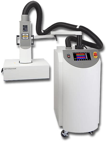
- Investing in test equipment: Acquire specialized HALT-HASS chambers and vibration tables capable of generating the required stress levels and accurately monitoring the test conditions.
- Training personnel: Ensure that engineers and technicians are well-versed in HALT-HASS principles, test procedures, and data analysis techniques to effectively conduct the tests and interpret the results.
- Integrating with product development and manufacturing processes: Incorporate HALT-HASS into the overall product development and manufacturing workflow, ensuring seamless communication and feedback loops between design, testing, and production teams.
Conducting HALT Tests
A typical HALT test for telecom PCB assemblies involves the following steps:
- Baseline testing: Perform initial functional tests to establish a performance baseline before applying environmental stresses.
- Thermal stress testing: Subject the assembly to rapid temperature cycling, gradually increasing the temperature range and ramp rates until a failure occurs or the test limits are reached.
- Vibration stress testing: Apply random, multi-axis vibration to the assembly, increasing the intensity until a failure occurs or the test limits are reached.
- Combined stress testing: Simultaneously apply thermal and vibration stresses to identify any interactions between failure modes.
- Failure analysis: Investigate the root causes of any failures observed during the test and determine the necessary design improvements.
- Design optimization: Implement the identified design changes and repeat the HALT test to validate the improvements.
| Stress Type | Typical Stress Levels |
|---|---|
| Temperature Cycling | -80°C to +125°C, ramp rates up to 60°C/min |
| Vibration | 10-50 Grms, 2-5,000 Hz, 6 DOF |
| Combined Stress | Temperature cycling and vibration applied simultaneously |
Implementing HASS Screening
Once the product design has been optimized through HALT, HASS screening is implemented in the manufacturing process to ensure the consistency and reliability of production units. A typical HASS screening process for telecom PCB assemblies includes:
- Defining screening levels: Determine the environmental stress levels for HASS based on the product’s operating limits and the destruct limits established during HALT.
- Setting up the HASS chamber: Configure the HASS chamber to apply the required stress levels and monitor the test conditions.
- Screening production units: Subject each production unit to the HASS screening process, which typically involves a combination of thermal cycling and vibration stress.
- Monitoring and data analysis: Continuously monitor the performance of the PCB assemblies during the screening process and analyze the data to identify any latent defects or manufacturing issues.
- Addressing manufacturing issues: Investigate and address any issues identified during HASS screening, such as component quality problems or process inconsistencies.
| Parameter | Typical HASS Screening Levels |
|---|---|
| Temperature Cycling | -40°C to +85°C, ramp rates up to 30°C/min |
| Vibration | 5-20 Grms, 2-2,000 Hz, 6 DOF |
| Duration | 4-48 hours, depending on product complexity and reliability requirements |

The Impact of HALT-HASS on Telecom PCB Assembly Reliability
Implementing HALT-HASS testing methodologies in the development and manufacturing of telecom PCB assemblies has a significant impact on product reliability and customer satisfaction. By exposing design weaknesses and latent manufacturing defects early in the process, HALT-HASS enables manufacturers to deliver more robust and reliable products to the market.
Improved Product Quality and Reliability
HALT-HASS helps improve the overall quality and reliability of telecom PCB assemblies by:
- Identifying and addressing design weaknesses: HALT reveals design flaws and component limitations, allowing engineers to optimize the product design for robustness and reliability.
- Screening out manufacturing defects: HASS identifies latent manufacturing defects, ensuring that only high-quality, reliable units are shipped to customers.
- Reducing field failures and warranty claims: By addressing issues early in the development and manufacturing process, HALT-HASS helps minimize the occurrence of costly field failures and warranty claims.
Accelerated Time-to-Market
HALT-HASS testing methodologies can help accelerate the time-to-market for new telecom products by:
- Identifying design issues early: HALT reveals design weaknesses early in the development process, allowing engineers to make necessary changes before committing to mass production.
- Reducing the need for lengthy field trials: By subjecting PCB assemblies to accelerated environmental stresses, HALT-HASS can provide valuable insights into product reliability in a shorter time frame compared to traditional field trials.
- Streamlining the manufacturing process: HASS screening helps identify and address manufacturing issues quickly, reducing production delays and improving overall process efficiency.
Cost Savings and Competitive Advantage
Investing in HALT-HASS testing can lead to significant cost savings and competitive advantages for telecom equipment manufacturers:
- Reduced warranty and repair costs: By improving product reliability and reducing field failures, HALT-HASS helps minimize warranty and repair expenses.
- Lower manufacturing costs: Identifying and addressing manufacturing issues early in the process helps reduce scrap, rework, and production downtime, leading to lower overall manufacturing costs.
- Enhanced customer satisfaction and loyalty: Delivering high-quality, reliable products that meet or exceed customer expectations helps build trust and loyalty, leading to increased market share and revenue growth.

Frequently Asked Questions (FAQ)
- What is the difference between HALT and HASS?
-
HALT (Highly Accelerated Life Testing) is used during the product development phase to identify design weaknesses and component limitations by subjecting the product to extreme environmental stresses. HASS (Highly Accelerated Stress Screening) is employed during the manufacturing process to screen for latent defects and ensure the consistency and reliability of production units.
-
How does HALT-HASS testing benefit telecom PCB assemblies?
-
HALT-HASS testing helps improve the reliability and durability of telecom PCB assemblies by identifying design weaknesses, screening out manufacturing defects, and ensuring that the products can withstand the rigors of long-term use in harsh environments. This leads to reduced field failures, lower warranty costs, and enhanced customer satisfaction.
-
What types of environmental stresses are applied during HALT-HASS testing?
-
HALT-HASS testing typically involves subjecting PCB assemblies to a combination of environmental stresses, such as rapid temperature cycling, random multi-axis vibration, and combined temperature and vibration stress. The stress levels are gradually increased until the product fails or the test limits are reached.
-
How does HALT-HASS testing accelerate time-to-market for new telecom products?
-
HALT-HASS testing helps identify design issues early in the development process, reducing the need for lengthy field trials and allowing engineers to make necessary changes before committing to mass production. Additionally, HASS screening helps streamline the manufacturing process by quickly identifying and addressing production issues.
-
What are the long-term benefits of investing in HALT-HASS testing for telecom equipment manufacturers?
- Investing in HALT-HASS testing can lead to significant long-term benefits for telecom equipment manufacturers, including reduced warranty and repair costs, lower manufacturing expenses, improved product reliability and customer satisfaction, and increased market share and revenue growth.

Conclusion
HALT-HASS testing methodologies play a crucial role in ensuring the reliability and durability of telecom PCB assemblies. By subjecting these assemblies to extreme environmental stresses, HALT helps identify design weaknesses and component limitations, enabling engineers to optimize product designs for robustness. HASS screening, on the other hand, helps identify and address latent manufacturing defects, ensuring that only high-quality, reliable units are shipped to customers.
Implementing HALT-HASS in the development and manufacturing of telecom PCB assemblies offers numerous benefits, including improved product quality and reliability, accelerated time-to-market, and significant cost savings. By investing in these advanced testing methodologies, telecom equipment manufacturers can gain a competitive edge in the market, enhance customer satisfaction, and drive long-term business success.
As the telecommunications industry continues to evolve and demand ever-increasing levels of product performance and reliability, the importance of HALT-HASS testing will only continue to grow. Manufacturers that embrace these methodologies and integrate them into their product development and manufacturing processes will be well-positioned to meet the challenges of the future and deliver the high-quality, reliable products that customers demand.


Leave a Reply