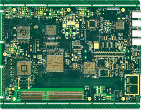
Introduction to Multilayer PCB
A Multilayer PCB, also known as a multilayer printed circuit board, is a complex and advanced type of PCB that consists of multiple layers of conductive copper foil laminated together with insulating material. These layers are interconnected through plated holes called vias, which allow electrical signals to pass between the different layers. Multilayer PCBs offer several advantages over traditional single or double-layer boards, including increased circuit density, improved signal integrity, and better electromagnetic interference (EMI) shielding.
Key Features of Multilayer PCBs
- Multiple layers of copper foil and insulating material
- Interconnected through plated holes (vias)
- Increased circuit density and complexity
- Improved signal integrity and EMI Shielding
- Used in a wide range of applications, from consumer electronics to aerospace
Multilayer PCB Manufacturing Process
The manufacturing process for multilayer PCBs is more complex and involves several steps compared to single or double-layer boards. The main stages of the multilayer PCB manufacturing process are:
-
Design and Layout: The first step is to create a detailed design and layout of the multilayer PCB using specialized software. This includes determining the number of layers, the placement of components, and the routing of traces.
-
Material Selection: The next step is to select the appropriate materials for the PCB, including the type of copper foil, insulating material, and solder mask. The choice of materials depends on the specific requirements of the application, such as temperature range, mechanical stress, and electrical properties.
-
Layer Preparation: Each layer of the multilayer PCB is prepared separately. This involves printing the circuit pattern onto the copper foil using a photoresist and then etching away the unwanted copper to create the traces and pads.
-
Lamination: The prepared layers are then stacked together with insulating material between them and laminated under high pressure and temperature to create a solid board.
-
Drilling: Holes are drilled through the laminated board to create vias that interconnect the different layers. The holes are then plated with copper to ensure electrical continuity.
-
Surface Finishing: The final step is to apply a surface finish to the PCB to protect the copper traces and pads from oxidation and to improve solderability. Common surface finishes include HASL (Hot Air Solder Leveling), ENIG (Electroless Nickel Immersion Gold), and OSP (Organic Solderability Preservative).
| Step | Description |
|---|---|
| Design and Layout | Create a detailed design and layout using specialized software |
| Material Selection | Select appropriate materials based on application requirements |
| Layer Preparation | Print circuit pattern and etch unwanted copper on each layer |
| Lamination | Stack layers with insulating material and laminate under high pressure and temperature |
| Drilling | Drill holes and plate with copper to create vias |
| Surface Finishing | Apply surface finish to protect copper and improve solderability |

Advantages of Multilayer PCBs
Multilayer PCBs offer several advantages over traditional single or double-layer boards, making them a popular choice for a wide range of applications. Some of the key advantages of multilayer PCBs are:
Increased Circuit Density
By using multiple layers, multilayer PCBs can accommodate a much higher number of components and traces in a smaller area compared to single or double-layer boards. This allows for more complex and compact designs, which is especially important in applications where space is limited, such as smartphones, wearables, and aerospace systems.
Improved Signal Integrity
Multilayer PCBs can provide better signal integrity by reducing crosstalk and noise between adjacent traces. By carefully designing the layout and using techniques such as ground planes and shielding layers, designers can minimize electromagnetic interference (EMI) and ensure reliable signal transmission.
Enhanced Thermal Management
Multilayer PCBs can also help with thermal management by providing more efficient heat dissipation. By using dedicated layers for power and ground planes, designers can create low-impedance paths for heat to flow away from components and prevent overheating.
Reduced Assembly Time and Cost
By integrating multiple layers into a single board, multilayer PCBs can reduce the number of separate boards and interconnects required for a given application. This can simplify assembly, reduce manufacturing time and cost, and improve overall reliability.

Applications of Multilayer PCBs
Multilayer PCBs are used in a wide range of applications across various industries, from consumer electronics to industrial automation and aerospace systems. Some of the common applications of multilayer PCBs include:
Consumer Electronics
Multilayer PCBs are extensively used in consumer electronics devices such as smartphones, tablets, laptops, and wearables. These devices require high component density, reliable performance, and compact size, making multilayer PCBs an ideal choice.
Automotive Electronics
Modern vehicles rely heavily on electronic systems for various functions such as engine control, infotainment, and advanced driver assistance systems (ADAS). Multilayer PCBs are used in these systems to provide reliable and robust performance in harsh environmental conditions.
Medical Devices
Medical devices such as pacemakers, implantable defibrillators, and imaging systems require high reliability, precision, and miniaturization. Multilayer PCBs are used in these devices to ensure accurate and reliable performance while meeting strict regulatory requirements.
Aerospace and Defense
Aerospace and defense applications demand the highest levels of reliability, performance, and environmental resistance. Multilayer PCBs are used in avionics, satellite systems, and military equipment to provide robust and reliable operation in extreme conditions.
Industrial Automation
Industrial automation systems such as programmable logic controllers (PLCs), human-machine interfaces (HMIs), and sensors rely on multilayer PCBs for reliable and efficient operation in harsh industrial environments.
| Application | Key Requirements | Benefits of Multilayer PCBs |
|---|---|---|
| Consumer Electronics | High density, reliable performance, compact size | Enables complex and compact designs |
| Automotive Electronics | Reliable and robust performance in harsh conditions | Provides reliable operation in challenging environments |
| Medical Devices | High reliability, precision, and miniaturization | Ensures accurate and reliable performance while meeting regulatory requirements |
| Aerospace and Defense | Highest levels of reliability, performance, and environmental resistance | Provides robust and reliable operation in extreme conditions |
| Industrial Automation | Reliable and efficient operation in harsh environments | Enables reliable operation in challenging industrial settings |

Frequently Asked Questions (FAQ)
1. What is the difference between a multilayer PCB and a single or double-layer PCB?
A multilayer PCB consists of three or more layers of conductive copper foil laminated together with insulating material, while a single or double-layer PCB has only one or two layers of copper foil. Multilayer PCBs offer higher circuit density, improved signal integrity, and better EMI shielding compared to single or double-layer boards.
2. How many layers can a multilayer PCB have?
Multilayer PCBs can have anywhere from 4 to over 50 layers, depending on the complexity of the design and the application requirements. However, most common multilayer PCBs have between 4 and 12 layers.
3. What materials are used in the construction of multilayer PCBs?
Multilayer PCBs are typically made of copper foil for the conductive layers, and a variety of insulating materials such as FR-4, Rogers, or polyimide for the substrate. The choice of materials depends on the specific requirements of the application, such as temperature range, mechanical stress, and electrical properties.
4. What are vias in a multilayer PCB, and what is their purpose?
Vias are plated holes that interconnect the different layers of a multilayer PCB. They allow electrical signals to pass between the layers, enabling more complex and compact circuit designs. There are several types of vias, including through-hole, blind, and buried vias, each serving a specific purpose in the PCB design.
5. What are the main advantages of using multilayer PCBs in electronic devices?
The main advantages of using multilayer PCBs in electronic devices include increased circuit density, improved signal integrity, enhanced thermal management, and reduced assembly time and cost. These benefits make multilayer PCBs a popular choice for a wide range of applications, from consumer electronics to aerospace systems.
Conclusion
Multilayer PCBs are a critical component in modern electronic devices, offering numerous advantages over traditional single or double-layer boards. By leveraging multiple layers of conductive and insulating materials, multilayer PCBs enable more complex and compact designs, improve signal integrity, and enhance thermal management. The manufacturing process for multilayer PCBs is more complex and involves several steps, including design and layout, material selection, layer preparation, lamination, drilling, and surface finishing. Multilayer PCBs find applications in various industries, such as consumer electronics, automotive, medical devices, aerospace, and industrial automation, where they provide reliable and robust performance in challenging environments. As electronic devices continue to become more sophisticated and compact, the importance of multilayer PCBs in enabling these advancements will only continue to grow.


Leave a Reply