Introduction to Surface Mount Technology
Surface Mount Technology (SMT) is a method for constructing electronic circuits in which the components are mounted directly onto the surface of a Printed Circuit Board (PCB). The electronic components used in this process are called Surface Mount Devices (SMDs). SMT has largely replaced the through-hole technology construction method, revolutionizing the electronics manufacturing industry by enabling the production of smaller, faster, and more cost-effective electronic devices.
Benefits of Surface Mount Technology
- Smaller component sizes
- Increased circuit density
- Faster assembly process
- Lower production costs
- Improved mechanical performance
Understanding Surface Mount Devices (SMDs)
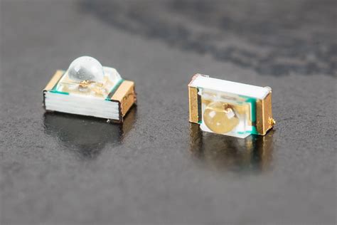
SMDs are electronic components designed for use in surface mount technology. These components are typically smaller than their through-hole counterparts and have either small leads or no leads at all. Instead, they have small metal pads, pins, or balls that are soldered directly onto the surface of the PCB.
Common Types of SMDs
- Resistors
- Capacitors
- Inductors
- Diodes
- Transistors
- Integrated Circuits (ICs)
SMD Package Types
SMDs come in various package types, each with its own size, shape, and pin configuration. Some common SMD package types include:
| Package Type | Description | Example Components |
|---|---|---|
| 0201 | Smallest SMD package, measuring 0.02″ x 0.01″ | Resistors, Capacitors |
| 0402 | Slightly larger than 0201, measuring 0.04″ x 0.02″ | Resistors, Capacitors |
| 0603 | Popular choice for resistors and capacitors | Resistors, Capacitors |
| 0805 | Larger than 0603, easier to handle | Resistors, Capacitors |
| 1206 | Largest common package for resistors and capacitors | Resistors, Capacitors |
| SOT | Small Outline Transistor, various sizes available | Transistors |
| SOIC | Small Outline Integrated Circuit | ICs |
| QFP | Quad Flat Pack, various sizes available | ICs |
| BGA | Ball Grid Array | ICs, Memory Modules |

Advantages of Using SMDs
Space Savings
One of the primary advantages of using SMDs is the significant space savings they offer compared to through-hole components. SMDs are much smaller, allowing for higher component density on a PCB. This enables the design of more compact electronic devices, such as smartphones, tablets, and wearables.
Improved Performance
SMDs offer improved electrical performance compared to through-hole components. The smaller size of SMDs reduces the parasitic capacitance and inductance, allowing for higher frequency operation and reduced signal distortion. This is particularly important in high-speed digital circuits and RF applications.
Cost Reduction
The use of SMDs can lead to significant cost reductions in electronics manufacturing. SMDs are less expensive than their through-hole counterparts, and the automated assembly process using pick-and-place machines is faster and more efficient. This results in lower labor costs and higher production throughput.
Enhanced Mechanical Reliability
SMDs have a lower profile and are more securely attached to the PCB compared to through-hole components. This enhances the mechanical reliability of the electronic device, making it more resistant to vibration and shock. The smaller size of SMDs also reduces the risk of component damage during handling and assembly.

SMD Assembly Process
The SMD assembly process involves several key steps to ensure proper placement and soldering of components onto the PCB.
Solder Paste Application
The first step in the SMD assembly process is the application of solder paste to the PCB. Solder paste is a mixture of tiny solder particles suspended in a flux medium. The paste is applied to the PCB using a stencil printing process, ensuring precise deposition of the paste onto the component pads.
Component Placement
Once the solder paste is applied, the SMDs are placed onto the PCB using a pick-and-place machine. These machines use vacuum nozzles or grippers to pick up the components from reels or trays and place them accurately on the PCB. Modern pick-and-place machines are highly automated and can place thousands of components per hour with great precision.
Reflow Soldering
After component placement, the PCB undergoes a reflow soldering process. The PCB is passed through a reflow oven, which heats the board to a specific temperature profile. The heat melts the solder paste, creating a permanent electrical and mechanical connection between the components and the PCB. The reflow process is carefully controlled to ensure optimal solder joint formation and to prevent component damage.
Inspection and Testing
Following the reflow soldering process, the assembLED PCB undergoes visual inspection and electrical testing to ensure proper component placement, solder joint quality, and circuit functionality. Automated optical inspection (AOI) systems are often used to detect placement errors, solder defects, and other manufacturing issues. Electrical testing verifies that the circuit performs as intended and meets the specified requirements.

Design Considerations for SMDs
When designing electronic circuits using SMDs, several factors must be considered to ensure optimal performance, reliability, and manufacturability.
PCB Layout
Proper PCB layout is crucial for the successful implementation of SMDs. The layout must account for the specific requirements of SMDs, such as pad size, spacing, and orientation. The PCB designer must also consider signal integrity, power distribution, and thermal management when placing SMDs on the board.
Thermal Management
SMDs can generate significant amounts of heat, particularly in high-power applications. Proper thermal management is essential to prevent component damage and ensure reliable operation. This can be achieved through careful component placement, the use of thermal vias, and the incorporation of heat sinks or other cooling methods.
Solder Joint Reliability
The reliability of solder joints is critical for the long-term performance of SMD-based electronic devices. Factors such as component size, pad design, and solder paste selection can impact solder joint reliability. Designers must follow best practices and industry standards to ensure robust and reliable solder joints.
Manufacturing Considerations
When designing with SMDs, it is important to consider the manufacturing process and the capabilities of the assembly facilities. This includes factors such as component availability, pick-and-place machine limitations, and reflow oven profiles. Designers should collaborate closely with the manufacturing team to ensure that the design is optimized for manufacturability and cost-effectiveness.
FAQs
Q1: Can SMDs be soldered by hand?
A1: While it is possible to hand solder SMDs, it can be challenging due to their small size and close spacing. Hand soldering SMDs requires a steady hand, good eyesight, and specialized tools such as fine-tipped Soldering Irons and tweezers. For most production applications, automated assembly using pick-and-place machines and reflow soldering is preferred.
Q2: Are SMDs more expensive than through-hole components?
A2: In general, SMDs are less expensive than their through-hole counterparts. The smaller size of SMDs allows for more efficient use of materials, and the automated assembly process reduces labor costs. However, the initial investment in SMT Assembly equipment can be higher than for through-hole assembly.
Q3: Can SMDs be replaced if they fail?
A3: Yes, SMDs can be replaced if they fail, but the process can be more challenging than replacing through-hole components. Replacing SMDs requires specialized tools, such as hot-air rework stations and microscopes, and a skilled technician. In some cases, it may be more cost-effective to replace the entire PCB rather than attempting to replace individual SMDs.
Q4: What is the smallest SMD package size?
A4: The smallest commonly used SMD package size is 0201, which measures 0.02″ x 0.01″ (0.5mm x 0.25mm). Some manufacturers offer even smaller packages, such as 01005 (0.4mm x 0.2mm), but these are less common and more challenging to work with.
Q5: Are there any disadvantages to using SMDs?
A5: While SMDs offer many advantages, there are a few potential disadvantages to consider:
1. SMDs can be more difficult to prototype and rework compared to through-hole components.
2. The small size of SMDs can make manual assembly and inspection more challenging.
3. Some SMD Packages, such as BGA, can be more difficult to inspect and repair than others.
4. The initial investment in SMT assembly equipment can be higher than for through-hole assembly.
Despite these potential drawbacks, the benefits of using SMDs, such as space savings, improved performance, and cost reduction, often outweigh the disadvantages in most modern electronic designs.
Conclusion
Surface Mount Devices (SMDs) have revolutionized the electronics manufacturing industry, enabling the production of smaller, faster, and more cost-effective electronic devices. By understanding the advantages, assembly process, and design considerations associated with SMDs, engineers and manufacturers can harness the full potential of this technology to create innovative and reliable electronic products.
As electronic devices continue to evolve and become more complex, the use of SMDs will remain essential for meeting the demands of the market. By staying informed about the latest advancements in SMT and SMD technology, designers and manufacturers can stay ahead of the curve and create products that push the boundaries of what is possible in the world of electronics.


Leave a Reply