History of Printed Circuit Boards
The concept of printed circuits can be traced back to the early 20th century. In 1903, Albert Hanson, a German inventor, filed a patent for a method of creating conductive pathways on an insulating material. However, it wasn’t until the 1940s that PCBs began to gain widespread use.
During World War II, the U.S. military required a more reliable and compact method of assembling electronic circuits for radar and radio equipment. In response, the National Bureau of Standards (now known as the National Institute of Standards and Technology) developed a process for printing conductive ink onto a ceramic substrate. This technique, known as “printed wiring,” laid the foundation for modern PCBs.
In the 1950s, the introduction of photo-etching techniques and the use of copper-clad laminates further advanced PCB technology. By the 1960s, PCBs had become the standard method for assembling electronic circuits in both military and consumer applications.
PCB Manufacturing Process
The manufacturing process for PCBs involves several steps, each of which contributes to the quality and reliability of the final product.
1. Design and Layout
The first step in creating a PCB is to design the circuit and lay out the components on the board. This is typically done using specialized software, such as Altium Designer or Eagle CAD. The designer must consider factors such as component placement, trace width and spacing, and signal integrity to ensure the board functions as intended.
2. Printing the Circuit Pattern
Once the design is finalized, the circuit pattern is printed onto the copper-clad laminate. This is typically done using a photoresist process, where a light-sensitive polymer is applied to the copper surface and exposed to UV light through a photomask containing the circuit pattern. The exposed areas of the photoresist harden, while the unexposed areas can be washed away, leaving the desired circuit pattern.
3. Etching
After the circuit pattern is printed, the board undergoes an etching process to remove the unwanted copper. The board is immersed in an etchant solution, such as ferric chloride or ammonium persulfate, which dissolves the exposed copper, leaving only the desired traces.
4. Drilling
Holes are drilled into the board to accommodate through-hole components and provide electrical connections between layers in multi-layer boards. This is typically done using computer-controlled drill machines.
5. Plating
To ensure reliable electrical connections and protect the copper traces from oxidation, the board is plated with a thin layer of metal, usually tin-lead alloy or gold. This process also deposits metal into the drilled holes, creating conductive pathways between layers.
6. Solder Mask and Silkscreen
A solder mask, usually green in color, is applied to the board to protect the copper traces from accidental solder bridges and provide insulation. A silkscreen layer is then added to print component labels, logos, and other identifying information on the board.
7. Surface Finishing
Finally, the exposed copper areas, such as contact pads and connector fingers, receive a surface finish to enhance solderability and protect against corrosion. Common surface finishes include Hot Air Solder Leveling (HASL), Electroless Nickel Immersion Gold (ENIG), and Organic Solderability Preservative (OSP).

Types of PCBs
PCBs can be classified based on the number of layers, the type of material used, and the manufacturing process.
Single-layer PCBs
Single-layer PCBs have conductive traces on only one side of the board. They are the simplest and most cost-effective type of PCB, suitable for low-complexity circuits and prototyping.
Double-layer PCBs
Double-layer PCBs have conductive traces on both sides of the board, with conductive vias connecting the layers. They offer higher component density and more design flexibility than single-layer boards.
Multi-layer PCBs
Multi-layer PCBs consist of three or more conductive layers separated by insulating layers. They are used for complex, high-density circuits that require a large number of interconnections, such as those found in smartphones, computers, and aerospace applications.
| Type | Layers | Complexity | Cost | Applications |
|---|---|---|---|---|
| Single-layer | 1 | Low | Low | Simple circuits, prototyping |
| Double-layer | 2 | Medium | Medium | More complex circuits, low-volume |
| Multi-layer | 3+ | High | High | High-density, complex circuits |
Rigid PCBs
Rigid PCBs are made from a solid, inflexible substrate material, such as FR-4 fiberglass. They are the most common type of PCB and are used in a wide range of applications.
Flexible PCBs
Flexible PCBs, or flex circuits, are made from a thin, flexible polymer film, such as polyimide. They can bend and fold to fit into tight spaces or conform to curved surfaces, making them ideal for applications with limited space or moving parts, such as cameras, wearables, and automobiles.
Rigid-Flex PCBs
Rigid-flex PCBs combine the benefits of both rigid and flexible PCBs. They consist of rigid sections connected by flexible sections, allowing for three-dimensional assembly and improved reliability in applications with vibration or shock.

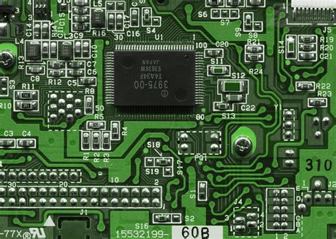
PCB Components
PCBs are designed to accommodate a wide variety of electronic components, each serving a specific function in the overall circuit.
Passive Components
Passive components are those that do not require a power source to operate and do not have the ability to control current flow. Examples include:
- Resistors: Control current flow and voltage levels
- Capacitors: Store and release electrical energy, filter signals
- Inductors: Store energy in magnetic fields, filter signals
Active Components
Active components are those that can control current flow and require a power source to operate. Examples include:
- Transistors: Amplify or switch electronic signals
- Diodes: Allow current to flow in only one direction
- Integrated Circuits (ICs): Perform complex functions, such as processing, memory, and communication
Connectors
Connectors provide a means of connecting the PCB to external devices or other PCBs. They come in various types, such as:
- Through-hole connectors: Pins are inserted into drilled holes and soldered
- Surface-mount connectors: Mounted directly onto the PCB surface
- Edge connectors: Conductive pads along the edge of the PCB mate with a socket

PCB Design Considerations
When designing a PCB, several factors must be considered to ensure optimal performance, reliability, and manufacturability.
Signal Integrity
Signal integrity refers to the ability of a signal to maintain its quality as it travels through the PCB. Factors that can affect signal integrity include:
- Trace length and width
- Impedance matching
- Crosstalk between adjacent traces
- Electromagnetic interference (EMI)
Designers must carefully route traces and place components to minimize these effects and ensure reliable signal transmission.
Power Distribution
Proper power distribution is crucial for the stable operation of the circuit. Designers must consider factors such as:
- Voltage drop across traces
- Current carrying capacity of traces
- Power plane design for low-impedance power delivery
- Decoupling capacitors to reduce power supply noise
Thermal Management
As electronic components generate heat during operation, effective thermal management is necessary to prevent overheating and ensure long-term reliability. Designers can use techniques such as:
- Proper component placement to distribute heat evenly
- Thermal vias to conduct heat away from components
- Heatsinks and cooling fans for high-power components
Manufacturing Constraints
PCB designers must also consider the limitations and requirements of the manufacturing process. These include:
- Minimum trace width and spacing
- Minimum drill hole size
- Clearance and creepage distances
- Solder mask and silkscreen requirements
Adhering to these constraints ensures that the PCB can be manufactured reliably and cost-effectively.
PCB Assembly
Once the PCB has been manufactured, the components must be assembled onto the board to create a functional circuit. There are two primary methods of PCB assembly: through-hole and surface-mount.
Through-hole Assembly
In through-hole assembly, component leads are inserted into drilled holes on the PCB and soldered to pads on the opposite side. This method is well-suited for larger components and provides a strong mechanical connection. However, it is less space-efficient and more labor-intensive than surface-mount assembly.
Surface-mount Assembly
Surface-mount assembly involves placing components directly onto pads on the PCB surface and soldering them in place. This method allows for smaller component sizes, higher component density, and faster automated assembly. Surface-mount technology (SMT) has largely replaced through-hole assembly in modern electronics manufacturing.
Automated Assembly
PCB assembly is typically performed using automated equipment, such as pick-and-place machines and reflow ovens. These machines can quickly and accurately place components onto the board and solder them in place, enabling high-volume production.
Testing and Quality Control
To ensure the reliability and functionality of the assembled PCB, various testing and quality control measures are employed.
Visual Inspection
Visual inspection is the first step in quality control, where the assembled PCB is examined for defects such as:
- Solder bridges or cold solder joints
- Misaligned or missing components
- Damaged or lifted pads
- Contamination or debris
Automated Optical Inspection (AOI)
AOI uses cameras and image processing software to automatically detect assembly defects, such as missing or misplaced components, solder defects, and incorrect component polarity. AOI systems can quickly inspect large numbers of boards, making them an essential tool in high-volume production.
In-Circuit Testing (ICT)
ICT involves using a bed-of-nails fixture to make electrical contact with specific points on the PCB and test the functionality of individual components and circuits. This method can detect defects such as:
- Open or short circuits
- Incorrect component values
- Missing or damaged components
Functional Testing
Functional testing involves subjecting the assembled PCB to its intended operating conditions and verifying that it performs as expected. This may include:
- Power-on testing
- Signal integrity testing
- Environmental stress testing (e.g., temperature, humidity, vibration)
Functional testing ensures that the PCB meets its design specifications and is ready for integration into the final product.
Applications of PCBs
PCBs are used in virtually every electronic device, from consumer electronics to industrial and aerospace systems. Some common applications include:
- Computers and peripherals
- Smartphones and tablets
- Televisions and home entertainment systems
- Automotive electronics
- Medical devices
- Industrial control systems
- Aerospace and defense systems
As technology advances, PCBs continue to evolve to meet the demands of new applications, such as the Internet of Things (IoT), 5G communication, and artificial intelligence (AI).
Future of PCBs
The future of PCBs is driven by the ever-increasing demand for smaller, faster, and more complex electronic devices. Some key trends shaping the future of PCBs include:
Miniaturization
As devices become smaller and more portable, PCBs must also shrink in size. This requires the use of advanced materials, such as high-density interconnect (HDI) substrates, and new manufacturing techniques, such as embedded components and 3D printing.
High-speed and High-frequency
With the growth of 5G communication and other high-speed applications, PCBs must be designed to handle higher frequencies and data rates. This requires the use of advanced materials with low dielectric constants and careful attention to signal integrity and EMI.
Sustainability
As environmental concerns grow, there is an increasing focus on sustainable PCB manufacturing practices. This includes the use of lead-free solders, halogen-free materials, and recyclable substrates, as well as the adoption of energy-efficient manufacturing processes.
Flexible and Wearable Electronics
The demand for flexible and wearable electronics, such as smartwatches and medical sensors, is driving the development of new PCB technologies. These include stretchable and conformable substrates, as well as the integration of PCBs with textiles and other materials.
Frequently Asked Questions (FAQ)
- What is the difference between a PCB and a breadboard?
-
A PCB is a permanent, custom-designed board with etched copper traces that connect components. A breadboard is a temporary prototyping tool with spring-loaded clips that allow components to be easily inserted and removed for testing and experimentation.
-
Can PCBs be repaired?
-
Yes, PCBs can be repaired, but the feasibility and cost-effectiveness of the repair depend on the extent of the damage and the complexity of the board. Common repair techniques include soldering, trace repair, and component replacement.
-
How long do PCBs last?
-
The lifespan of a PCB depends on various factors, such as the quality of the materials, the manufacturing process, and the operating environment. With proper design and manufacturing, a PCB can last for many years or even decades.
-
What is the difference between a solder mask and a silkscreen?
-
A solder mask is a protective layer applied to the PCB to prevent solder bridges and provide insulation between traces. A silkscreen is a printed layer that contains component labels, logos, and other identifying information.
-
What is the most common material used for PCB substrates?
- FR-4, a glass-reinforced epoxy laminate, is the most widely used material for PCB substrates due to its excellent mechanical and electrical properties, as well as its cost-effectiveness.
In conclusion, PCBs are essential components in modern electronics, providing a reliable and efficient means of interconnecting electronic components. As technology continues to advance, PCBs will play an increasingly crucial role in enabling new and innovative applications.


Leave a Reply