How PCB Stencils Work
PCB stencils work by providing a uniform layer of solder paste on the PCB pads. The stencil is placed on top of the PCB, and solder paste is spread across the stencil using a squeegee. The solder paste passes through the openings in the stencil and is deposited onto the corresponding pads on the PCB. After the stencil is removed, the PCB is ready for component placement and reflow soldering.
The thickness of the stencil and the size of the openings determine the amount of solder paste applied to each pad. This is critical because too much or too little solder paste can lead to defects such as bridging, insufficient solder joints, or tombstoning.
Stencil Thickness
The thickness of a PCB stencil is typically measured in mils (thousandths of an inch) or microns. Common stencil thicknesses range from 3-8 mils (75-200 microns), depending on the size and pitch of the components being used. A thicker stencil will deposit more solder paste, which is suitable for larger components or pads. Conversely, a thinner stencil is better for smaller components and fine-pitch applications.
| Component Size | Pitch | Recommended Stencil Thickness |
|---|---|---|
| 1005 (0402) | 0.5 mm | 3-4 mils (75-100 microns) |
| 0603 | 0.8 mm | 4-5 mils (100-125 microns) |
| 0805 | 1.27 mm | 5-6 mils (125-150 microns) |
| 1206 | 1.27 mm | 6-7 mils (150-175 microns) |
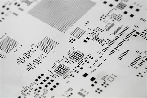
Aperture Design
The openings in the stencil, known as apertures, are designed to match the size and shape of the pads on the PCB. The aperture design is crucial for ensuring the correct amount of solder paste is deposited on each pad. Factors that influence aperture design include:
- Pad size and shape
- Solder paste type and viscosity
- Component pitch and density
- Stencil thickness
Apertures can be simple rectangles, circles, or more complex shapes, depending on the pad geometry. In some cases, apertures may be slightly larger than the pad to account for solder paste shrinkage during reflow.
Stencil Materials
PCB stencils can be made from various materials, each with its own advantages and disadvantages. The most common materials are:
-
Stainless Steel: Durable, long-lasting, and suitable for high-volume production. Stainless steel stencils offer excellent print definition and are easy to clean.
-
Polyester: Lower cost and suitable for prototyping or low-volume production. Polyester stencils are less durable than stainless steel but offer good print quality.
-
Nickel: Similar properties to stainless steel but with added corrosion resistance. Nickel stencils are suitable for high-volume production and challenging environments.

Stencil Frame Types
PCB stencils are typically mounted in a frame to provide stability and ease of handling during the solder paste application process. There are several types of stencil frames, including:
-
Standard Frame: A simple, cost-effective solution suitable for most applications. Standard frames are available in various sizes and materials, such as aluminum or stainless steel.
-
Frameless: A space-saving option that eliminates the need for a separate frame. Frameless stencils are held in place by the solder paste printer’s clamping system.
-
Stepped Frame: Designed for PCBs with components on both sides. Stepped frames allow for different stencil thicknesses on each side of the PCB, accommodating the varying component heights.
-
Tensioned Frame: Uses a tensioning system to keep the stencil taut, minimizing distortion and improving print quality. Tensioned frames are suitable for high-precision applications.

Stencil Cleaning and Maintenance
Regular cleaning and maintenance of PCB stencils are essential for ensuring consistent print quality and extending the stencil’s lifespan. Solder paste residue can accumulate on the stencil, causing blockages in the apertures and inconsistent solder paste deposits.
Stencils should be cleaned immediately after use with a suitable solvent, such as isopropyl alcohol (IPA) or a specialized stencil cleaning solution. Manual cleaning with a lint-free wipe or automated stencil cleaning systems can be used, depending on the production volume and available resources.
Proper storage of PCB stencils is also important to prevent damage and contamination. Stencils should be stored in a clean, dry environment, away from direct sunlight and excessive humidity. Protective covers or containers can be used to shield the stencils from dust and debris.

Advantages of Using PCB Stencils
Using PCB stencils offers several advantages in the electronic manufacturing process:
-
Consistency: Stencils ensure a uniform solder paste deposit on each pad, reducing the risk of defects caused by insufficient or excessive solder.
-
Efficiency: Stencil printing is a fast and efficient method for applying solder paste to PCBs, making it suitable for high-volume production.
-
Precision: Laser-cut stencils provide high precision and repeatability, ensuring accurate solder paste placement on even the smallest pads.
-
Cost-effective: While the initial investment in a stencil may be higher than other solder paste application methods, the long-term benefits of reduced defects and increased efficiency make it a cost-effective solution.
Challenges and Considerations
Despite the many advantages of using PCB stencils, there are some challenges and considerations to keep in mind:
-
Design Complexity: As PCBs become more complex, with finer pitches and smaller components, stencil design becomes more challenging. Ensuring the correct aperture size and shape for each pad requires careful planning and collaboration between the PCB designer and stencil manufacturer.
-
Stencil Wear: Over time, stencils can become worn or damaged, leading to inconsistent solder paste deposits. Regular inspection and replacement of stencils are necessary to maintain print quality.
-
Solder Paste Selection: The type and viscosity of solder paste used can affect the print quality and the stencil’s performance. It’s essential to select a solder paste that is compatible with the stencil and the specific application.
-
Stencil Alignment: Proper alignment of the stencil to the PCB is crucial for accurate solder paste deposition. Misalignment can lead to defects such as bridging or insufficient solder joints. Automated solder paste printers with vision systems can help ensure precise alignment.
Frequently Asked Questions (FAQ)
-
What is the difference between a PCB stencil and a Solder Paste Mask?
A PCB stencil is a separate, reusable tool used to apply solder paste to the PCB pads. A solder paste mask, on the other hand, is a layer of the PCB itself that defines the areas where solder paste should be applied. The solder paste mask is typically made of a non-conductive material and is permanently applied to the PCB during the manufacturing process. -
Can I use the same stencil for different PCB designs?
In most cases, each PCB design will require its own unique stencil. The stencil apertures must match the size, shape, and location of the pads on the specific PCB. However, if you have multiple PCB designs with identical pad layouts, you may be able to use the same stencil for those designs. -
How often should I clean my PCB stencil?
The frequency of cleaning depends on the volume of production and the type of solder paste being used. In general, it’s a good practice to clean the stencil after every print cycle or at least once per shift. However, if you notice a decline in print quality or excessive solder paste buildup, more frequent cleaning may be necessary. -
What is the typical lifespan of a PCB stencil?
The lifespan of a PCB stencil depends on several factors, including the material, thickness, and frequency of use. Stainless steel stencils are the most durable and can last for tens of thousands of print cycles with proper care and maintenance. Polyester stencils have a shorter lifespan, typically lasting a few thousand print cycles. -
Can I use a PCB stencil for hand soldering?
While PCB stencils are primarily used in automated solder paste printing processes, they can also be used for hand soldering. Applying solder paste through a stencil can help ensure consistent and precise solder paste deposition, even when hand soldering. However, the stencil must be carefully aligned with the PCB and secured in place to prevent shifting during the solder paste application process.
In conclusion, PCB stencils are a critical tool in the electronic manufacturing process, enabling precise and consistent solder paste application for high-quality solder joints. By understanding the various aspects of PCB stencils, including materials, aperture design, and maintenance requirements, manufacturers can optimize their soldering processes and produce reliable, high-performance electronic devices.


Leave a Reply