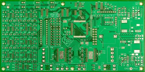
Introduction to Round PCBs
Round PCBs are printed circuit boards that have a circular shape instead of the traditional rectangular or square shape. They are commonly used in applications where space is limited, such as wearable devices, smart watches, and medical equipment. Round PCBs offer several advantages, including:
- Compact size and efficient use of space
- Aesthetic appeal and unique design possibilities
- Improved mechanical stability and durability
Despite their benefits, designing round PCBs requires careful consideration of various factors to ensure optimal performance and manufacturability.
PCB design Considerations for Round Boards
1. Board Size and Shape
When designing a round PCB, the first consideration is the size and shape of the board. The diameter of the board should be determined based on the available space and the components that need to be accommodated. It is important to ensure that the board size is sufficient to accommodate all the necessary components while maintaining adequate spacing and clearance.
| Board Diameter | Typical Applications |
|---|---|
| < 20 mm | Wearable devices, small sensors |
| 20 – 50 mm | Smart watches, medical devices |
| 50 – 100 mm | Industrial sensors, automotive components |
| > 100 mm | Specialized applications, large-scale projects |
2. Component Placement
Component placement on a round PCB requires careful planning to optimize space utilization and minimize signal integrity issues. The following guidelines should be considered:
- Place components symmetrically around the center of the board to maintain balance and stability
- Group related components together to minimize the length of traces and improve signal integrity
- Avoid placing components too close to the edge of the board to prevent mechanical stress and damage
- Consider the orientation of components to facilitate assembly and minimize the risk of tombstoning
3. Trace Routing
Trace routing on a round PCB can be challenging due to the limited space and the need to maintain signal integrity. The following guidelines should be followed:
- Use curved traces instead of sharp angles to minimize signal reflections and improve signal quality
- Maintain consistent trace width and spacing to ensure impedance control and reduce crosstalk
- Avoid crossing traces whenever possible to minimize electromagnetic interference (EMI)
- Use via-in-pad or blind vias to optimize space utilization and improve routing efficiency
4. Power and Ground Planes
Proper power and ground plane design is crucial for ensuring stable power delivery and minimizing noise in a round PCB. Consider the following guidelines:
- Use solid power and ground planes to provide low-impedance paths for current flow
- Maintain adequate clearance between power and ground planes to prevent short circuits
- Use multiple power and ground layers to improve current carrying capacity and reduce voltage drop
- Implement proper decoupling and bypass capacitors to minimize power supply noise and ensure stable voltage levels
5. Manufacturability and Assembly
Designing a round PCB with manufacturability and assembly in mind is essential to ensure a smooth production process. Consider the following guidelines:
- Adhere to the manufacturer’s design rules and specifications for minimum trace width, spacing, and hole sizes
- Provide sufficient clearance around the edge of the board for panelization and depanelization processes
- Include fiducial marks and alignment holes to facilitate accurate component placement during assembly
- Consider the assembly process, such as reflow soldering or wave soldering, and design the board accordingly
Frequently Asked Questions (FAQs)
1. What are the advantages of using a round PCB over a rectangular PCB?
Round PCBs offer several advantages, including compact size, efficient space utilization, aesthetic appeal, and improved mechanical stability. They are particularly suitable for applications where space is limited or where a unique design is desired.
2. How do I determine the appropriate size for my round PCB?
The size of your round PCB should be determined based on the available space in your application and the components that need to be accommodated. Consider the diameter of the board and ensure that there is sufficient space for all the necessary components while maintaining adequate spacing and clearance.
3. What are the challenges in routing traces on a round PCB?
Routing traces on a round PCB can be challenging due to the limited space and the need to maintain signal integrity. It is important to use curved traces, maintain consistent trace width and spacing, avoid crossing traces, and utilize via-in-pad or blind vias to optimize routing efficiency.
4. How can I ensure proper power and ground plane design in a round PCB?
To ensure proper power and ground plane design in a round PCB, use solid planes to provide low-impedance paths for current flow, maintain adequate clearance between planes, use multiple layers for improved current carrying capacity, and implement proper decoupling and bypass capacitors to minimize noise and ensure stable voltage levels.
5. What are the manufacturability considerations for round PCBs?
When designing a round PCB for manufacturability, adhere to the manufacturer’s design rules and specifications, provide sufficient clearance around the edge of the board for panelization and depanelization, include fiducial marks and alignment holes for accurate assembly, and consider the assembly process, such as reflow soldering or wave soldering, to ensure compatibility.

Conclusion
Designing round PCBs requires careful consideration of various factors, including board size and shape, component placement, trace routing, power and ground plane design, and manufacturability. By following the guidelines and best practices outlined in this article, you can create effective and reliable round PCBs that meet the specific requirements of your application.
When designing a round PCB, it is essential to collaborate closely with your PCB manufacturer and assembly partner to ensure that your design is optimized for production and meets all the necessary specifications. By taking a holistic approach to PCB design and considering all the relevant factors, you can create innovative and high-quality round PCBs that excel in both form and function.


Leave a Reply