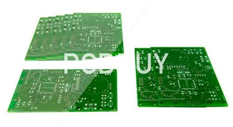
What is PCB Warpage?
PCB warpage is the deviation of a printed circuit board from its intended flat shape. It occurs when the board experiences uneven stress or thermal expansion, causing it to bend or twist. The severity of warpage can vary depending on various factors such as material properties, manufacturing processes, and environmental conditions.
Types of PCB Warpage
There are two main types of PCB warpage:
-
Bow: This type of warpage occurs when the PCB curves along its length or width, forming an arc-like shape.
-
Twist: Twist warpage happens when the PCB twists along its diagonal axis, resulting in a corkscrew-like shape.
The following table illustrates the differences between bow and twist warpage:
| Warpage Type | Description | Illustration |
|---|---|---|
| Bow | PCB curves along its length or width | |
| Twist | PCB twists along its diagonal axis |
Causes of PCB Warpage
Several factors can contribute to PCB warpage. Understanding these causes is crucial for preventing and mitigating the issue.
Material Properties
The choice of materials used in PCB Fabrication plays a significant role in warpage. Different materials have varying coefficients of thermal expansion (CTE), which determine how much they expand or contract when subjected to temperature changes. When materials with mismatched CTEs are used together, it can lead to uneven stress distribution and warpage.
Some common PCB materials and their CTEs are listed in the table below:
| Material | CTE (ppm/°C) |
|---|---|
| FR-4 | 14-17 |
| Polyimide | 12-16 |
| Aluminum | 23-24 |
| Copper | 17 |
Manufacturing Processes
The manufacturing processes involved in PCB fabrication can also contribute to warpage. Uneven heating or cooling during soldering, lamination, or reflow processes can cause thermal stress, leading to warpage. Additionally, improper handling or storage of PCBs during manufacturing can introduce mechanical stress, resulting in distortion.
Environmental Conditions
Environmental factors such as temperature, humidity, and pressure can influence PCB warpage. Exposure to extreme temperatures or rapid temperature changes can cause the board to expand or contract unevenly, leading to warpage. High humidity levels can also affect the moisture content of the PCB materials, causing them to swell or deform.

Effects of PCB Warpage
PCB warpage can have several detrimental effects on the functionality and reliability of electronic devices.
Component Placement Issues
Warped PCBs can pose challenges during the component placement process. Surface mount components may not sit flush on the board, leading to poor soldering and potential connectivity issues. Through-hole components may not align properly with the holes, making it difficult to insert them correctly.
Soldering Defects
Warpage can cause soldering defects such as bridging, tombstoning, or open circuits. When the PCB is not flat, components may not make proper contact with the solder pads, resulting in weak or incomplete solder joints. This can lead to reliability issues and even device failure.
Mechanical Stress
Warped PCBs can experience increased mechanical stress, particularly in areas with high component density or heavy components. The uneven distribution of stress can cause cracks, delamination, or fractures in the board, compromising its structural integrity.
Reduced Reliability
The cumulative effects of component placement issues, soldering defects, and mechanical stress can significantly impact the overall reliability of the electronic device. Warped PCBs are more prone to failures, reduced performance, and shorter lifespans.

Preventing PCB Warpage
To minimize the occurrence of PCB warpage, several preventive measures can be taken during the design and manufacturing stages.
Material Selection
Careful selection of PCB materials is crucial for reducing warpage. Consider using materials with similar CTEs to minimize thermal stress. For example, using a substrate material with a CTE close to that of copper can help reduce warpage caused by thermal expansion mismatches.
Design Considerations
During the PCB design phase, consider the following guidelines to mitigate warpage:
- Use symmetrical layer stackups to balance the stress distribution across the board.
- Avoid abrupt changes in copper density, as they can lead to uneven thermal expansion.
- Incorporate stress-relief features such as slots or cutouts in high-stress areas.
- Minimize the use of large, heavy components that can exert excessive mechanical stress on the board.
Manufacturing Process Optimization
Optimizing the manufacturing processes can help reduce warpage:
- Implement controlled heating and cooling cycles during soldering and lamination to minimize thermal stress.
- Use appropriate support structures or fixtures to keep the PCB flat during reflow or Wave Soldering.
- Ensure proper handling and storage of PCBs to avoid mechanical stress or deformation.
- Regularly calibrate and maintain manufacturing equipment to ensure consistent and uniform processes.
Quality Control and Inspection
Implementing rigorous quality control and inspection procedures can help identify and address warpage issues early in the manufacturing process. Use automated optical inspection (AOI) systems or 3D scanning techniques to measure and monitor PCB flatness. Establish acceptable warpage thresholds and reject boards that exceed these limits.

FAQ
-
What is the difference between bow and twist warpage?
Bow warpage occurs when the PCB curves along its length or width, forming an arc-like shape. Twist warpage happens when the PCB twists along its diagonal axis, resulting in a corkscrew-like shape. -
Can PCB warpage be completely eliminated?
While it may not be possible to completely eliminate PCB warpage, it can be minimized through careful material selection, design considerations, manufacturing process optimization, and quality control measures. -
How does PCB warpage affect component placement?
Warped PCBs can cause component placement issues, such as surface mount components not sitting flush on the board or through-hole components not aligning properly with the holes. This can lead to poor soldering and potential connectivity issues. -
What role does material selection play in preventing PCB warpage?
Selecting PCB materials with similar coefficients of thermal expansion (CTE) can help reduce warpage caused by thermal stress. Using a substrate material with a CTE close to that of copper is one example of how material selection can mitigate warpage. -
How can quality control and inspection help address PCB warpage?
Implementing rigorous quality control and inspection procedures, such as automated optical inspection (AOI) or 3D scanning, can help identify and address warpage issues early in the manufacturing process. Establishing acceptable warpage thresholds and rejecting boards that exceed these limits can ensure that only flat PCBs are used in the final product.
Conclusion
PCB warpage is a complex issue that can have significant impacts on the functionality, reliability, and longevity of electronic devices. By understanding the causes, effects, and prevention methods of warpage, manufacturers and designers can take proactive steps to minimize its occurrence.
Effective prevention of PCB warpage requires a holistic approach that encompasses material selection, design considerations, manufacturing process optimization, and quality control measures. By addressing warpage at various stages of the PCB lifecycle, manufacturers can ensure the production of high-quality, reliable electronic products.
As the electronics industry continues to evolve, with increasing demands for miniaturization and higher performance, managing PCB warpage will remain a critical aspect of successful product development. Staying informed about the latest advancements in materials, design techniques, and manufacturing processes will be essential for staying ahead of the curve in the ever-changing landscape of PCB fabrication.


Leave a Reply