What is PCB Warpage?
PCB warpage, also known as PCB bow and twist, is a common issue that occurs during the manufacturing process of printed circuit boards (PCBs). It refers to the distortion or deviation from flatness of the PCB, which can cause various problems in the assembly and functionality of the final product. PCB warpage can manifest in two main forms: bow and twist.
Bow
Bow is a type of warpage where the PCB curves along its length or width, forming an arc-like shape. It is measured as the maximum distance between the PCB surface and a flat reference plane. Bow can occur in either a concave or convex direction, depending on the stresses and conditions the PCB is subjected to during manufacturing.
Twist
Twist, on the other hand, is a type of warpage where the PCB rotates along its diagonal axis, resulting in one corner of the board being higher or lower than the others. Twist is measured as the maximum distance between the highest and lowest corners of the PCB relative to a flat reference plane.
Causes of PCB Warpage
There are several factors that can contribute to PCB warpage during the manufacturing process. Understanding these causes is crucial for preventing or minimizing warpage in PCBs.
Thermal Stress
One of the primary causes of PCB warpage is thermal stress. During the manufacturing process, PCBs are subjected to high temperatures, especially during the soldering and reflow stages. The different materials used in the PCB, such as the substrate, copper layers, and solder mask, have different coefficients of thermal expansion (CTE). When exposed to heat, these materials expand and contract at different rates, leading to internal stresses within the PCB. If these stresses are not properly managed, they can cause the PCB to warp.
Moisture Absorption
Moisture absorption is another common cause of PCB warpage. PCBs are often exposed to humid environments during storage, transportation, and assembly. The substrate material, typically FR-4, is hygroscopic, meaning it can absorb moisture from the surrounding environment. When the PCB is subjected to high temperatures, such as during soldering or reflow, the absorbed moisture can vaporize and cause the PCB to expand and warp.
Uneven Copper Distribution
The distribution of copper on the PCB can also contribute to warpage. If the copper layers are not evenly distributed across the board, it can lead to unbalanced stresses. Areas with higher copper density will have different thermal expansion rates compared to areas with lower copper density, resulting in localized warpage.
Improper Handling and Storage
Improper handling and storage of PCBs can also cause warpage. If PCBs are not stored in a flat and stable condition, they can develop a permanent bow or twist over time. Additionally, mishandling during the assembly process, such as applying excessive force or bending the board, can lead to warpage.

Effects of PCB Warpage
PCB warpage can have several negative effects on the functionality and reliability of the final product.
Assembly Challenges
Warped PCBs can pose significant challenges during the assembly process. If the PCB is not flat, it can be difficult to align and place components accurately on the board. This can lead to misaligned or poorly soldered components, resulting in electrical failures or reduced reliability.
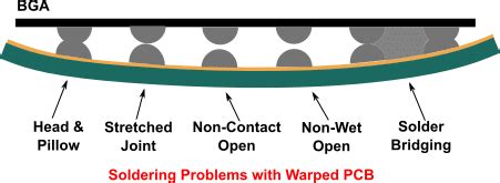
Soldering Defects
Warpage can also cause soldering defects, such as bridging, insufficient solder joints, or open circuits. When the PCB is warped, it can create uneven surfaces that prevent proper contact between the components and the solder pads. This can result in weak or incomplete solder joints, compromising the electrical integrity of the board.
Mechanical Stress
Warped PCBs can experience increased mechanical stress, especially when subjected to vibration or physical shock. The uneven distribution of stress across the board can lead to cracks, delamination, or component failure over time.
Reduced Reliability
The combination of assembly challenges, soldering defects, and mechanical stress can significantly reduce the overall reliability of the PCB and the final product. Warped PCBs are more likely to experience premature failures or malfunction, leading to increased warranty claims and customer dissatisfaction.

Preventing PCB Warpage
To minimize the occurrence of PCB warpage, several preventive measures can be taken during the design and manufacturing process.
Material Selection
Selecting appropriate materials for the PCB substrate and components is crucial for reducing warpage. Using materials with similar CTEs can help minimize the internal stresses caused by thermal expansion differences. For example, using a high-Tg (Glass Transition Temperature) substrate material can improve the PCB’s resistance to warpage at elevated temperatures.
Balanced Copper Distribution
Ensuring a balanced distribution of copper on the PCB can help prevent localized warpage. During the design phase, it is important to consider the placement and density of copper features, such as traces and planes. Techniques like copper balancing and symmetric design can help distribute the copper evenly across the board.
Moisture Management
To prevent warpage caused by moisture absorption, proper moisture management techniques should be implemented. PCBs should be stored in a dry environment with controlled humidity levels. Before subjecting the PCBs to high temperatures, such as during soldering or reflow, it is essential to perform a pre-bake process to remove any absorbed moisture.
Proper Handling and Storage
Implementing proper handling and storage procedures can help prevent PCB warpage. PCBs should be stored in flat and stable conditions, preferably in specialized racks or trays designed to keep them flat. During the assembly process, care should be taken to avoid applying excessive force or bending the board.
Manufacturing Process Control
Controlling the manufacturing process parameters can also help minimize PCB warpage. This includes optimizing the temperature profiles during soldering and reflow, controlling the cooling rate to minimize thermal shock, and using appropriate fixtures and support structures to keep the PCB flat during processing.

Measuring and Inspecting PCB Warpage
Measuring and inspecting PCB warpage is important for quality control and ensuring the reliability of the final product. There are several methods and tools used to measure and quantify PCB warpage.
Visual Inspection
Visual inspection is a simple and quick method to identify gross warpage in PCBs. By placing the PCB on a flat surface and observing any visible deviation from flatness, operators can identify boards with excessive bow or twist. However, visual inspection is subjective and may not detect subtle warpage.
Flatness Gauges
Flatness gauges, such as feeler gauges or dial indicators, can be used to measure the distance between the PCB surface and a flat reference plane. These tools provide a quantitative measurement of the bow or twist, allowing for more accurate assessment of warpage.
3D Scanning
Advanced 3D scanning techniques, such as laser scanning or structured light scanning, can provide detailed surface measurements of the PCB. These methods generate a 3D model of the board, allowing for precise measurement of warpage and visualization of the distortion pattern.
Warpage Testing Standards
Several industry standards provide guidelines for measuring and specifying PCB warpage. IPC (Association Connecting Electronics Industries) has published standards such as IPC-TM-650 and IPC-A-610, which define methods for measuring and evaluating PCB flatness and warpage.
FAQ
1. What is the difference between bow and twist in PCB warpage?
Bow refers to the curvature of the PCB along its length or width, forming an arc-like shape. Twist, on the other hand, is the rotation of the PCB along its diagonal axis, resulting in one corner being higher or lower than the others.
2. What are the main causes of PCB warpage?
The main causes of PCB warpage include thermal stress, moisture absorption, uneven copper distribution, and improper handling and storage. These factors can lead to internal stresses and distortion of the PCB during the manufacturing process.
3. How does PCB warpage affect the assembly process?
Warped PCBs can pose challenges during the assembly process, making it difficult to align and place components accurately on the board. This can result in misaligned or poorly soldered components, leading to electrical failures or reduced reliability.
4. What preventive measures can be taken to minimize PCB warpage?
Preventive measures for minimizing PCB warpage include selecting appropriate materials with similar CTEs, ensuring a balanced distribution of copper, implementing proper moisture management techniques, following proper handling and storage procedures, and controlling the manufacturing process parameters.
5. How is PCB warpage measured and inspected?
PCB warpage can be measured and inspected using various methods, including visual inspection, flatness gauges, and 3D scanning techniques. Industry standards, such as those published by IPC, provide guidelines for measuring and evaluating PCB flatness and warpage.
| Warpage Type | Description | Measurement |
|---|---|---|
| Bow | Curvature of the PCB along its length or width | Maximum distance between PCB surface and flat reference |
| Twist | Rotation of the PCB along its diagonal axis | Maximum distance between highest and lowest corners |
Table 1: Types of PCB Warpage
| Cause | Description |
|---|---|
| Thermal Stress | Different CTE of materials leading to internal stresses |
| Moisture Absorption | Substrate absorbing moisture and expanding during heating |
| Uneven Copper Distribution | Unbalanced stresses due to uneven copper density |
| Improper Handling/Storage | PCBs developing permanent warpage due to improper conditions |
Table 2: Causes of PCB Warpage
| Prevention Measure | Description |
|---|---|
| Material Selection | Using materials with similar CTE to minimize thermal stresses |
| Balanced Copper Distribution | Evenly distributing copper features across the PCB |
| Moisture Management | Storing PCBs in dry environment and performing pre-bake |
| Proper Handling/Storage | Storing PCBs in flat and stable conditions |
| Process Control | Optimizing manufacturing parameters to minimize warpage |
Table 3: Prevention Measures for PCB Warpage
In conclusion, understanding and addressing PCB warpage is crucial for ensuring the quality, reliability, and functionality of printed circuit boards. By recognizing the causes, effects, and preventive measures related to bow and twist, designers and manufacturers can take proactive steps to minimize warpage and improve the overall performance of their PCBs.


Leave a Reply