Introduction to PCB Prototyping
PCB prototyping is an essential step in the development of electronic devices. It involves creating a physical representation of a printed circuit board (PCB) design to test its functionality, compatibility, and performance before mass production. In this article, we will explore the top myths and facts about PCB prototyping and assembly to help you better understand the process and make informed decisions.
What is PCB Prototyping?
PCB prototyping is the process of creating a small batch of printed circuit boards based on a specific design. The purpose of prototyping is to verify the design, test the functionality, and ensure that the PCB meets the required specifications before proceeding with mass production. Prototyping allows designers and engineers to identify and fix any issues early in the development process, saving time and money in the long run.
The PCB Prototyping Process
The PCB prototyping process typically involves the following steps:
-
Design: The PCB design is created using specialized software, such as Altium Designer, Eagle, or KiCad. The design includes the schematic, component placement, and routing of the traces.
-
Fabrication: Once the design is finalized, the PCB Prototype is fabricated using various methods, such as milling, etching, or 3D printing. The choice of fabrication method depends on the complexity of the design, the required turnaround time, and the available budget.
-
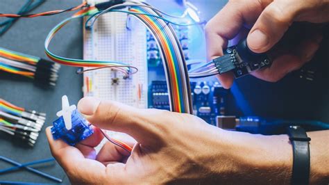
Assembly: After fabrication, the components are soldered onto the PCB prototype. This can be done manually or using automated assembly processes, such as pick-and-place machines and reflow ovens.
-
Testing: The assembled PCB prototype is then tested to ensure that it functions as intended. This may involve functional testing, boundary scan testing, and in-circuit testing, among others.
-
Iteration: Based on the test results, the PCB design may be modified, and the prototyping process is repeated until the desired performance and functionality are achieved.

Myths about PCB Prototyping
Despite the importance of PCB prototyping, there are several misconceptions that can lead to poor design decisions and increased costs. Let’s debunk some of the most common myths about PCB prototyping.
Myth 1: Prototyping is Expensive and Time-Consuming
One of the most prevalent myths about PCB prototyping is that it is an expensive and time-consuming process. While it is true that prototyping requires an initial investment, it can actually save you money and time in the long run by identifying and addressing issues early in the development process.
Fact: PCB prototyping can help you avoid costly mistakes and delays in mass production by allowing you to test and refine your design before committing to large-scale manufacturing.
Myth 2: Prototyping is Only Necessary for Complex Designs
Another common myth is that PCB prototyping is only necessary for complex or high-density designs. However, even simple designs can benefit from prototyping, as it allows you to verify the functionality and compatibility of the components and ensure that the PCB meets the required specifications.
Fact: PCB prototyping is valuable for designs of all complexities, as it helps to identify potential issues and optimize the design for manufacturability.
Myth 3: In-House Prototyping is Always Better
Some companies believe that in-house PCB prototyping is always better than outsourcing to a professional prototyping service. While in-house prototyping can provide more control over the process, it also requires significant investments in equipment, materials, and skilled personnel.
Fact: Outsourcing PCB prototyping to a reputable service provider can be more cost-effective and efficient, especially for companies with limited resources or expertise in PCB fabrication and assembly.

Facts about PCB Prototyping
Now that we have dispelled some of the common myths about PCB prototyping, let’s explore some essential facts that you should know.
Fact 1: Prototyping Enables Design Optimization
PCB prototyping allows designers to optimize their designs for manufacturability, reliability, and performance. By creating physical prototypes, designers can identify potential issues, such as signal integrity problems, thermal management challenges, and mechanical constraints, and make necessary adjustments before mass production.
Fact 2: Rapid Prototyping Accelerates Time-to-Market
Rapid prototyping techniques, such as 3D printing and laser cutting, have revolutionized the PCB prototyping process. These methods allow for faster turnaround times and more flexible design iterations, enabling companies to bring their products to market faster and stay ahead of the competition.
Fact 3: Prototyping Facilitates Collaboration and Communication
PCB prototyping facilitates collaboration and communication between design teams, manufacturers, and stakeholders. Physical prototypes provide a tangible representation of the design, making it easier to discuss and evaluate the product’s functionality, aesthetics, and user experience.

PCB Assembly Techniques
Once the PCB prototype has been fabricated, the next step is to assemble the components onto the board. There are several PCB assembly techniques, each with its own advantages and limitations.
Through-Hole Assembly
Through-hole assembly involves inserting component leads through drilled holes in the PCB and soldering them to pads on the opposite side. This technique is suitable for larger components and provides strong mechanical bonds, making it ideal for high-reliability applications.
Advantages:
– Strong mechanical bonds
– Suitable for larger components
– Easy to inspect and repair
Limitations:
– Requires drilling holes, which increases fabrication time and cost
– Consumes more board space compared to surface-mount assembly
Surface-Mount Assembly
Surface-mount assembly involves soldering components directly onto pads on the surface of the PCB. This technique allows for smaller component sizes and higher component density, making it suitable for compact and high-performance applications.
Advantages:
– Smaller component sizes and higher component density
– Faster assembly process
– Lower fabrication costs
Limitations:
– Requires precise placement and soldering equipment
– More challenging to inspect and repair compared to through-hole assembly
Mixed Assembly
Mixed assembly combines both through-hole and surface-mount techniques on the same PCB. This approach offers the benefits of both techniques and is suitable for applications that require a mix of component types and sizes.
Advantages:
– Combines the benefits of through-hole and surface-mount assembly
– Accommodates a wide range of component types and sizes
Limitations:
– Requires careful planning and design to ensure compatibility between the two techniques
– May increase fabrication and assembly complexity
PCB Prototyping and Assembly Best Practices
To ensure successful PCB prototyping and assembly, consider the following best practices:
-
Choose the Right Fabrication Method: Select a fabrication method that balances your design requirements, timeline, and budget. Consider factors such as design complexity, required precision, and material properties when making your choice.
-
Use Reliable Components: Ensure that the components used in your PCB prototype are of high quality and from reputable suppliers. Subpar components can lead to performance issues and reliability problems.
-
Follow Design for Manufacturing (DFM) Guidelines: Adhere to DFM guidelines to ensure that your PCB design is optimized for manufacturability. This includes considerations such as component placement, trace routing, and solder mask design.
-
Perform Thorough Testing: Conduct comprehensive testing of your PCB prototype to verify its functionality, performance, and reliability. This may include functional testing, environmental testing, and accelerated life testing, among others.
-
Work with Experienced Partners: Partner with experienced PCB prototyping and assembly service providers who have the expertise, equipment, and processes to deliver high-quality results. Look for providers with a proven track record and positive customer reviews.
Frequently Asked Questions (FAQ)
-
What is the typical turnaround time for PCB prototyping?
The turnaround time for PCB prototyping varies depending on the complexity of the design, the chosen fabrication method, and the service provider. Rapid prototyping techniques, such as 3D printing, can provide prototypes within a few days, while more complex designs may take several weeks. -
How much does PCB prototyping cost?
The cost of PCB prototyping depends on factors such as the size and complexity of the design, the chosen fabrication method, and the quantity of prototypes required. Rapid prototyping techniques may have higher per-unit costs but lower setup costs compared to traditional fabrication methods. -
What are the most common PCB prototyping fabrication methods?
The most common PCB prototyping fabrication methods include: - Milling: Removing unwanted copper from a pre-laminated board using a milling machine.
- Etching: Chemically removing unwanted copper from a pre-laminated board using a photoresist and etchant.
-
3D Printing: Additively manufacturing the PCB structure using conductive and insulating materials.
-
What are the advantages of outsourcing PCB prototyping and assembly?
Outsourcing PCB prototyping and assembly offers several advantages, including: - Access to specialized expertise and equipment
- Reduced capital investment in in-house resources
- Faster turnaround times and increased flexibility
-
Scalability to handle varying production volumes
-
How can I ensure the quality of my PCB prototype?
To ensure the quality of your PCB prototype, consider the following: - Choose reliable components and materials
- Follow DFM guidelines and industry standards
- Perform thorough testing and inspection
- Work with experienced and reputable prototyping and assembly partners
- Implement a robust quality control process
Conclusion
PCB prototyping and assembly are critical aspects of electronic product development. By understanding the myths and facts surrounding these processes, you can make informed decisions and optimize your designs for success. Remember to choose the right fabrication methods, use reliable components, follow best practices, and partner with experienced providers to ensure the quality and reliability of your PCB prototypes.
As technology continues to evolve, so do the techniques and tools available for PCB prototyping and assembly. Staying up-to-date with the latest advancements and trends will help you stay competitive and deliver innovative products to market faster.


Leave a Reply