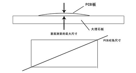
What is PCB Warpage?
PCB warpage is a common issue in the PCB assembly process where the printed circuit board deforms or bends, resulting in an uneven surface. This can lead to various problems, such as poor component placement, reduced reliability, and increased manufacturing costs. Understanding the causes of PCB warpage and implementing appropriate prevention measures is crucial for ensuring the quality and functionality of the final product.
Causes of PCB Warpage
1. Thermal Stress
One of the primary causes of PCB warpage is thermal stress. During the assembly process, PCBs are exposed to high temperatures, which can cause the board to expand and contract unevenly. This uneven expansion and contraction can lead to warpage, especially if the PCB has an asymmetrical design or if there are differences in the thermal expansion coefficients of the materials used.
2. Moisture Absorption
Moisture absorption is another significant factor contributing to PCB warpage. PCBs are often exposed to humid environments during storage, transportation, and assembly. When the board absorbs moisture, it can expand and cause warpage, particularly when subjected to high temperatures during the soldering process.
3. Unbalanced Copper Distribution
An unbalanced copper distribution on the PCB can also contribute to warpage. If there is a significant difference in the amount of copper on the top and bottom layers of the board, it can lead to uneven thermal expansion and contraction, resulting in warpage.
4. Inappropriate Material Selection
Choosing inappropriate materials for the PCB substrate and components can also cause warpage. Materials with different thermal expansion coefficients or those that are not compatible with the assembly process can lead to uneven expansion and contraction, resulting in warpage.
5. Mechanical Stress
Mechanical stress, such as bending or twisting of the PCB during handling or assembly, can also cause warpage. This is particularly true for thin or flexible PCBs, which are more susceptible to mechanical deformation.

Prevention Measures for PCB Warpage
1. Proper Material Selection
Choosing the right materials for the PCB substrate and components is crucial for preventing warpage. Materials should have similar thermal expansion coefficients and be compatible with the assembly process. For example, using a high-Tg (glass transition temperature) substrate can help reduce warpage caused by thermal stress.
2. Balanced Copper Distribution
Ensuring a balanced copper distribution on the PCB can help prevent warpage caused by uneven thermal expansion and contraction. This can be achieved by designing the board with symmetrical copper patterns and avoiding large copper pours on one side of the board.
3. Moisture Control
Controlling moisture absorption is essential for preventing PCB warpage. This can be done by storing PCBs in a dry environment, using moisture-barrier bags during transportation, and baking the boards before assembly to remove any absorbed moisture.
4. Optimized Thermal Profile
Developing an optimized thermal profile for the soldering process can help minimize thermal stress and reduce the risk of warpage. This involves carefully controlling the temperature ramp-up and cool-down rates, as well as the peak temperature and duration of exposure.
5. Proper Handling and Support
Proper handling and support of the PCB during assembly can help prevent mechanical stress and reduce the risk of warpage. This includes using appropriate fixtures and supports to keep the board flat and avoid bending or twisting during the assembly process.

Visualizing PCB Warpage Data
To better understand the impact of various factors on PCB warpage, it can be helpful to visualize the data in a table format. The following table shows the relationship between different causes and their relative contribution to PCB warpage:
| Cause | Relative Contribution |
|---|---|
| Thermal Stress | High |
| Moisture Absorption | Medium |
| Unbalanced Copper Distribution | Medium |
| Inappropriate Material Selection | High |
| Mechanical Stress | Low |
By understanding the relative contribution of each cause, manufacturers can prioritize their prevention efforts and focus on the most significant factors contributing to PCB warpage.

Frequently Asked Questions (FAQ)
-
What is the most common cause of PCB warpage?
The most common cause of PCB warpage is thermal stress, which occurs when the board is exposed to high temperatures during the assembly process, leading to uneven expansion and contraction. -
How can moisture absorption cause PCB warpage?
When a PCB absorbs moisture, it can expand and cause warpage, particularly when subjected to high temperatures during the soldering process. This is because the absorbed moisture vaporizes and exerts pressure on the board, leading to deformation. -
What materials are best suited for preventing PCB warpage?
Materials with similar thermal expansion coefficients and high glass transition temperatures (Tg) are best suited for preventing PCB warpage. Examples include FR-4 substrates with high Tg values and low-CTE (coefficient of thermal expansion) copper foils. -
How can an optimized thermal profile help prevent PCB warpage?
An optimized thermal profile helps prevent PCB warpage by carefully controlling the temperature ramp-up and cool-down rates, as well as the peak temperature and duration of exposure. This minimizes thermal stress on the board and reduces the risk of uneven expansion and contraction. -
What role does proper handling and support play in preventing PCB warpage?
Proper handling and support of the PCB during assembly is crucial for preventing mechanical stress and reducing the risk of warpage. This involves using appropriate fixtures and supports to keep the board flat and avoid bending or twisting during the assembly process.
Conclusion
PCB warpage is a significant issue in the PCB assembly process that can lead to various problems, such as poor component placement, reduced reliability, and increased manufacturing costs. By understanding the primary causes of PCB warpage, such as thermal stress, moisture absorption, unbalanced copper distribution, inappropriate material selection, and mechanical stress, manufacturers can implement effective prevention measures.
These measures include proper material selection, balanced copper distribution, moisture control, optimized thermal profiles, and proper handling and support during assembly. By prioritizing these prevention efforts and focusing on the most significant contributing factors, manufacturers can minimize the risk of PCB warpage and ensure the quality and functionality of their final products.


Leave a Reply