Introduction to PCB Plating Methods
Printed circuit boards (PCBs) are essential components in modern electronic devices. They provide the electrical connections and mechanical support for various components, such as integrated circuits, resistors, capacitors, and connectors. To ensure the reliability and functionality of PCBs, manufacturers employ various plating methods during the production process.
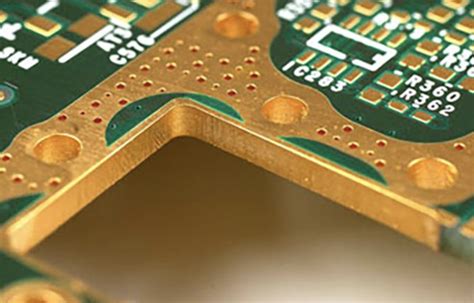
Plating is a crucial step in PCB manufacturing that involves depositing a thin layer of metal onto the surface of the board. This metal layer serves several purposes, including:
- Improving the electrical conductivity of the copper traces
- Protecting the copper from oxidation and corrosion
- Enhancing the solderability of the pads and through-holes
- Providing a smooth and uniform surface finish
In this article, we will explore the top four types of plating methods used in PCB manufacturing:
- Electroless Plating
- Electrolytic Plating
- Immersion Plating
- Organic Solderability Preservative (OSP) Coating
We will discuss the advantages, disadvantages, and applications of each method to help you understand their roles in producing high-quality PCBs.
Electroless Plating
Electroless plating, also known as chemical or autocatalytic plating, is a process that deposits a thin layer of metal onto the PCB surface without the use of an external electrical current. Instead, it relies on a chemical reduction reaction to deposit the metal ions onto the substrate.
How Electroless Plating Works
The electroless plating process involves the following steps:
-
Cleaning: The PCB surface is thoroughly cleaned to remove any contaminants or oxides that may interfere with the plating process.
-
Activation: The surface is treated with a catalytic solution, usually containing palladium or tin, to create a surface that is receptive to the plating solution.
-
Plating: The activated PCB is immersed in the electroless plating solution, which contains the metal ions (e.g., copper, nickel, or gold) and a reducing agent. The reducing agent chemically reduces the metal ions, causing them to deposit onto the catalytic surface of the PCB.
-
Rinsing: After plating, the PCB is rinsed with water to remove any excess plating solution and prevent further deposition.
Advantages of Electroless Plating
- Uniform deposition: Electroless plating produces a uniform metal layer, even on complex shapes and hard-to-reach areas.
- No electrical current required: Since electroless plating does not rely on an external electrical current, it can be used on non-conductive substrates or areas without electrical connections.
- Excellent adhesion: The chemical bond between the deposited metal and the substrate results in strong adhesion.
- Versatility: Electroless plating can deposit various metals, such as copper, nickel, and gold, depending on the application requirements.
Disadvantages of Electroless Plating
- Slower deposition rate: Compared to electrolytic plating, electroless plating has a slower deposition rate, which can impact production throughput.
- Higher material costs: The chemicals used in electroless plating, particularly the reducing agents and catalysts, can be more expensive than those used in other plating methods.
- Environmental concerns: Some electroless plating solutions contain harmful chemicals that require proper handling, disposal, and wastewater treatment.
Applications of Electroless Plating in PCB Manufacturing
Electroless plating is commonly used for the following applications in PCB manufacturing:
- Through-hole plating: Electroless copper plating is used to create a conductive layer inside the through-holes of the PCB, ensuring reliable electrical connections between layers.
- Soldermask adhesion: A thin layer of electroless copper is often applied before the soldermask to improve its adhesion to the PCB surface.
- Surface finish: Electroless nickel/immersion gold (ENIG) is a popular surface finish that provides excellent solderability, corrosion resistance, and shelf life.

Electrolytic Plating
Electrolytic plating, also known as electroplating, is a process that uses an electric current to deposit a layer of metal onto the PCB surface. It involves the transfer of metal ions from an anode to the PCB (cathode) through an electrolyte solution.
How Electrolytic Plating Works
The electrolytic plating process consists of the following steps:
-
Cleaning: As with electroless plating, the PCB surface is cleaned to remove contaminants and oxides.
-
Electrolyte preparation: An electrolyte solution containing the dissolved metal ions (e.g., copper, nickel, or gold) is prepared. The composition and concentration of the electrolyte depend on the desired plating characteristics.
-
Anode and cathode setup: The PCB is connected as the cathode, while a metal anode (usually the same metal as the one being plated) is placed in the electrolyte solution.
-
Plating: An electric current is applied between the anode and cathode, causing the metal ions to migrate from the anode to the PCB surface, where they are reduced and deposited as a thin metal layer.
-
Rinsing: After plating, the PCB is rinsed with water to remove any excess electrolyte and prevent further deposition.
Advantages of Electrolytic Plating
- High deposition rate: Electrolytic plating offers a higher deposition rate compared to electroless plating, allowing for faster production times.
- Thickness control: By adjusting the current density and plating time, the thickness of the deposited metal layer can be precisely controlled.
- Cost-effectiveness: Electrolytic plating is generally more cost-effective than electroless plating due to lower material costs and higher production throughput.
- Wide range of metals: Electrolytic plating can deposit various metals, including copper, nickel, gold, silver, and tin.
Disadvantages of Electrolytic Plating
- Requires electrical conductivity: Electrolytic plating can only be applied to conductive surfaces, limiting its use on non-conductive substrates or areas without electrical connections.
- Non-uniform deposition: Electrolytic plating may result in non-uniform metal deposition, especially on complex shapes or high-aspect-ratio features, due to current density variations.
- Anode maintenance: The metal anode used in electrolytic plating needs to be regularly maintained or replaced to ensure consistent plating quality.
Applications of Electrolytic Plating in PCB Manufacturing
Electrolytic plating is widely used in PCB manufacturing for the following applications:
- Copper plating: Electrolytic copper plating is used to increase the thickness of the copper traces and pads, improving their current-carrying capacity and mechanical strength.
- Surface finish: Electrolytic nickel/gold (ENEG) and electrolytic tin are common surface finishes that provide good solderability and protection against oxidation.
- Via filling: Electrolytic copper plating is used to fill the vias in high-density interconnect (HDI) PCBs, creating reliable electrical connections between layers.

Immersion Plating
Immersion plating is a simple and cost-effective method that involves dipping the PCB into a plating solution containing the desired metal ions. Unlike electroless and electrolytic plating, immersion plating does not require an external catalyst or electrical current.
How Immersion Plating Works
The immersion plating process involves the following steps:
-
Cleaning: The PCB surface is cleaned to remove contaminants and oxides.
-
Immersion: The PCB is dipped into the plating solution, which contains the metal ions (e.g., tin, silver, or gold) and a complexing agent. The complexing agent helps to control the plating reaction and maintain the stability of the solution.
-
Displacement reaction: The metal ions in the solution undergo a displacement reaction with the copper on the PCB surface. The more noble metal (e.g., tin, silver, or gold) displaces the less noble copper, resulting in a thin metal layer on the PCB surface.
-
Rinsing: After plating, the PCB is rinsed with water to remove any excess plating solution and prevent further deposition.
Advantages of Immersion Plating
- Simplicity: Immersion plating is a simple and straightforward process that does not require complex equipment or setup.
- Cost-effectiveness: Compared to other plating methods, immersion plating is relatively inexpensive due to its simplicity and lower material costs.
- Uniform deposition: Immersion plating produces a uniform metal layer on the PCB surface, even on complex shapes and hard-to-reach areas.
- Suitable for non-conductive substrates: Since immersion plating does not rely on an external electrical current, it can be used on non-conductive substrates or areas without electrical connections.
Disadvantages of Immersion Plating
- Limited thickness: The metal layer deposited by immersion plating is typically thin (0.1-0.5 μm), as the displacement reaction is self-limiting. Thicker layers may require multiple plating cycles or alternative methods.
- Limited metal options: Immersion plating is mainly used for depositing noble metals, such as tin, silver, and gold, which can displace copper. Other metals may not be suitable for this method.
- Copper etching: During the displacement reaction, some of the copper on the PCB surface is etched away, which can lead to a slight decrease in the thickness of the copper traces and pads.
Applications of Immersion Plating in PCB Manufacturing
Immersion plating is commonly used for the following applications in PCB manufacturing:
- Surface finish: Immersion tin (ISn), immersion silver (IAg), and immersion gold (IGAu) are popular surface finishes that provide good solderability and protection against oxidation.
- Wire bondability: Immersion gold is often used as a surface finish for wire bonding pads, as it provides a clean and oxide-free surface for reliable wire bonding.
- Press-fit connectors: Immersion tin is sometimes used as a surface finish for press-fit connectors, as it provides a smooth and uniform surface for reliable mechanical and electrical contact.

Organic Solderability Preservative (OSP) Coating
Organic Solderability Preservative (OSP) coating is a non-metallic surface finish that protects the exposed copper on the PCB surface from oxidation and ensures good solderability. OSP is an alternative to metallic surface finishes, such as HASL, ENIG, or immersion tin.
How OSP Coating Works
The OSP coating process involves the following steps:
-
Cleaning: The PCB surface is thoroughly cleaned to remove contaminants and oxides.
-
OSP application: The PCB is dipped into or sprayed with an OSP solution, which contains organic compounds that form a protective layer on the copper surface. Common OSP formulations include benzimidazole, benzotriazole, and imidazole derivatives.
-
Drying: After OSP application, the PCB is dried using hot air or infrared heating to remove any excess solution and ensure a uniform coating.
Advantages of OSP Coating
- Cost-effectiveness: OSP coating is a cost-effective surface finish compared to metallic finishes, as it requires fewer processing steps and materials.
- Thin and uniform coating: OSP forms a thin (0.2-0.5 μm) and uniform coating on the copper surface, which does not significantly affect the dimensions of the PCB features.
- Good solderability: OSP provides good solderability by protecting the copper surface from oxidation and ensuring a clean surface for solder wetting.
- Environmentally friendly: OSP coating is generally considered an environmentally friendly surface finish, as it does not contain heavy metals or require hazardous waste treatment.
Disadvantages of OSP Coating
- Limited shelf life: OSP-coated PCBs have a limited shelf life (typically 6-12 months) compared to metallic surface finishes, as the organic coating can degrade over time, especially when exposed to high temperatures or humidity.
- Reduced multiple reflow capability: OSP coating may not withstand multiple reflow cycles as effectively as metallic surface finishes, which can impact the rework and repair processes.
- Incompatibility with some assembly processes: OSP coating may not be compatible with certain assembly processes, such as wire bonding or press-fit connectors, which require specific metallic surface finishes.
Applications of OSP Coating in PCB Manufacturing
OSP coating is commonly used for the following applications in PCB manufacturing:
- Consumer electronics: OSP is widely used in consumer electronics, where cost-effectiveness and good solderability are essential.
- Short production runs: OSP coating is suitable for short production runs or prototypes, as it does not require extensive setup or processing times.
- Lead-free assembly: OSP coating is compatible with lead-free soldering processes, as it can withstand higher reflow temperatures compared to some metallic surface finishes.
Comparison of PCB Plating Methods
To help you understand the differences between the four plating methods discussed in this article, we have created a comparison table:
| Plating Method | Deposition Mechanism | Thickness (μm) | Advantages | Disadvantages | Common Applications |
|---|---|---|---|---|---|
| Electroless Plating | Chemical reduction | 0.5-5 | Uniform deposition, no electrical current required, excellent adhesion | Slower deposition rate, higher material costs, environmental concerns | Through-hole plating, soldermask adhesion, ENIG surface finish |
| Electrolytic Plating | Electric current | 1-100 | High deposition rate, thickness control, cost-effectiveness | Requires electrical conductivity, non-uniform deposition, anode maintenance | Copper plating, ENEG surface finish, via filling |
| Immersion Plating | Displacement reaction | 0.1-0.5 | Simplicity, cost-effectiveness, uniform deposition | Limited thickness, limited metal options, copper etching | ISn, IAg, and IGAu surface finishes, wire bondability |
| OSP Coating | Organic compound adsorption | 0.2-0.5 | Cost-effectiveness, thin and uniform coating, good solderability, environmentally friendly | Limited shelf life, reduced multiple reflow capability, incompatibility with some assembly processes | Consumer electronics, short production runs, lead-free assembly |
FAQ
-
Q: Which plating method is the most cost-effective for high-volume PCB production?
A: Electrolytic plating is generally the most cost-effective method for high-volume PCB production due to its high deposition rate and lower material costs compared to electroless plating. -
Q: Can immersion plating be used for depositing thicker metal layers on PCBs?
A: Immersion plating typically results in thin metal layers (0.1-0.5 μm) due to the self-limiting nature of the displacement reaction. For thicker layers, multiple plating cycles or alternative methods, such as electrolytic plating, may be required. -
Q: Is OSP coating suitable for PCBs that require long-term storage before assembly?
A: OSP coating may not be the best choice for PCBs that require long-term storage, as the organic coating can degrade over time, especially when exposed to high temperatures or humidity. Metallic surface finishes, such as ENIG or immersion tin, are more suitable for long-term storage. -
Q: Which plating method is preferred for achieving the best soldermask adhesion?
A: Electroless copper plating is often used before applying the soldermask to improve its adhesion to the PCB surface. The thin layer of electroless copper provides a uniform and oxide-free surface for the soldermask to adhere to. -
Q: Can electrolytic plating be used on non-conductive substrates or areas without electrical connections?
A: No, electrolytic plating requires a conductive surface and an electrical connection to the area being plated. For non-conductive substrates or areas without electrical connections, electroless plating or immersion plating may be more suitable.
Conclusion
In summary, PCB plating methods play a crucial role in ensuring the reliability and functionality of printed circuit boards. Electroless plating, electrolytic plating, immersion plating, and OSP coating each have their own advantages, disadvantages, and applications in PCB manufacturing.
Choosing the most appropriate plating method depends on various factors, such as the desired surface finish, thickness requirements, production volume, cost considerations, and compatibility with assembly processes. By understanding the characteristics and capabilities of each plating method, PCB manufacturers can make informed decisions to produce high-quality PCBs that meet the specific requirements of their customers.
As technology advances and new materials emerge, PCB plating methods will continue to evolve to address the ever-growing demands of the electronics industry. Manufacturers must stay up-to-date with the latest developments in plating technologies to remain competitive and deliver cutting-edge PCB solutions to their customers.


Leave a Reply