Introduction to PCB Inkjet Printing
Printed Circuit Boards (PCBs) are essential components in modern electronics. They provide a platform for mounting and interconnecting electronic components, forming the backbone of almost all electronic devices. Traditionally, PCBs are manufactured using subtractive methods, such as etching or milling, which involve removing unwanted copper from a pre-coated board. However, these methods can be time-consuming, expensive, and environmentally unfriendly.
In recent years, inkjet printing has emerged as a promising alternative for PCB fabrication. By modifying a standard inkjet printer, it is possible to print conductive traces directly onto a substrate, creating a functional PCB. This method, known as PCB inkjet printing, offers several advantages over traditional manufacturing techniques, including faster prototyping, lower costs, and reduced environmental impact.
Benefits of PCB Inkjet Printing
- Rapid Prototyping: PCB inkjet printing allows for quick and easy creation of prototype boards, enabling faster iteration and testing of designs.
- Cost-Effective: Compared to traditional PCB manufacturing methods, inkjet printing requires less equipment and material, making it more affordable for small-scale production and hobbyists.
- Environmentally Friendly: Inkjet printing eliminates the need for harsh chemicals and reduces waste, making it a more eco-friendly option.
- Versatility: Inkjet printing can be used with a variety of substrates, including paper, plastic, and fabric, opening up new possibilities for flexible and wearable electronics.

Modifying an Inkjet Printer for PCB Printing
To begin printing PCBs using an inkjet printer, several modifications need to be made to the printer and its ink cartridges. The following steps outline the process of modifying an inkjet printer for PCB production:
Step 1: Choosing the Right Printer
When selecting an inkjet printer for PCB printing, consider the following factors:
- Compatibility with conductive ink cartridges
- Print resolution and accuracy
- Ease of modification
- Cost and availability of replacement parts
Some popular choices for PCB inkjet printing include the Epson Stylus series and the Canon PIXMA series.
Step 2: Preparing the Printer
Before making any modifications, it is essential to thoroughly clean the printer to remove any dust, debris, or dried ink that may interfere with the printing process. Follow these steps:
- Remove all ink cartridges and print heads from the printer.
- Clean the print head nozzles using a cleaning solution and soft brush.
- Flush the ink delivery system with distilled water to remove any remaining ink.
- Dry all components completely before reassembling the printer.
Step 3: Modifying the Ink Cartridges
To print conductive traces, the standard ink cartridges need to be replaced with cartridges containing conductive ink. There are two main options for obtaining conductive ink cartridges:
- Purchase pre-filled cartridges from a supplier specializing in conductive inks for inkjet printing.
- Refill empty cartridges with conductive ink using a syringe or ink refill kit.
When refilling cartridges, it is crucial to use a compatible conductive ink that is specifically formulated for inkjet printing. Some popular conductive inks include silver nanoparticle ink and graphene-based ink.
Step 4: Adjusting Printer Settings
To ensure optimal print quality and conductivity, adjust the following printer settings:
- Print Resolution: Set the print resolution to the highest setting available to achieve the best trace definition and minimize gaps in the printed traces.
- Ink Density: Increase the ink density to deposit more conductive material onto the substrate, improving conductivity.
- Print Speed: Reduce the print speed to allow the conductive ink to properly adhere to the substrate and minimize smearing or bleeding.
Step 5: Preparing the Substrate
For best results, use a substrate specifically designed for inkjet printing, such as inkjet printable PET film or photo paper. If using a non-standard substrate, ensure that it has a smooth, non-porous surface to prevent the ink from spreading or seeping into the material.
Before printing, clean the substrate with isopropyl alcohol to remove any oils, dust, or contaminants that may affect ink adhesion.

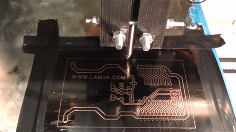
Designing and Printing PCBs
With the modified inkjet printer ready, the next step is to design and print the PCB. The following steps outline the process:
Step 1: PCB Design
Use PCB design software, such as KiCad or Eagle, to create the PCB layout. When designing the PCB for inkjet printing, consider the following factors:
- Trace Width: Ensure that the trace width is compatible with the resolution of the inkjet printer. A minimum trace width of 0.2 mm is recommended for most modified inkjet printers.
- Pad Size: Design pads that are large enough to accommodate the components and allow for some misalignment during printing.
- Layer Separation: If designing a multi-layer PCB, ensure adequate separation between layers to prevent short circuits.
Step 2: Print Settings and Calibration
Before printing the PCB, calibrate the printer and adjust the print settings to ensure optimal results:
- Align the print head to ensure accurate placement of the conductive ink.
- Perform a nozzle check to verify that all nozzles are functioning correctly.
- Adjust the print settings, such as resolution, ink density, and print speed, as determined in the previous section.
Step 3: Printing the PCB
Load the prepared substrate into the printer and initiate the print process. For best results, print multiple passes of the conductive ink to increase the thickness and conductivity of the traces.
After printing, allow the PCB to dry completely before handling or further processing. Some conductive inks may require additional curing or sintering to achieve optimal conductivity.

Post-Processing and Assembly
Once the PCB is printed and dried, several post-processing steps may be necessary before assembling the components:
Step 1: Curing or Sintering
Depending on the type of conductive ink used, the printed PCB may require additional curing or sintering to improve conductivity and durability. This can be achieved through various methods, such as:
- Heat curing: Expose the PCB to elevated temperatures (typically 100-200°C) for a specified duration to evaporate solvents and sinter the conductive particles.
- UV curing: Use ultraviolet light to cure the ink and enhance its electrical properties.
- Chemical sintering: Apply a chemical agent to the printed traces to promote sintering and improve conductivity.
Step 2: Insulation and Protection
To protect the printed traces from damage and prevent short circuits, apply a layer of insulation or protective coating over the PCB. Some options include:
- Solder mask: Apply a thin layer of solder mask to the PCB, leaving only the pads exposed for component assembly.
- Conformal coating: Use a spray-on or brush-on conformal coating to protect the PCB from moisture, dust, and other environmental factors.
Step 3: Component Assembly
After the PCB is cured and protected, proceed with assembling the components using standard soldering techniques. Be mindful of the temperature sensitivity of the printed traces and use a lower soldering temperature if necessary.
Troubleshooting and Optimization
When working with PCB inkjet printing, several common issues may arise. The following table provides solutions to some of these problems:
| Problem | Solution |
|---|---|
| Inconsistent or incomplete traces | – Clean the print head nozzles – Increase ink density – Print multiple passes |
| Poor ink adhesion | – Clean the substrate with isopropyl alcohol – Use a compatible substrate |
| Low conductivity | – Increase ink density – Print multiple passes – Optimize curing/sintering process |
| Smeared or blurred traces | – Reduce print speed – Ensure substrate is dry and clean |
To optimize the performance and reliability of printed PCBs, experiment with different ink formulations, substrate materials, and print settings to find the best combination for your specific application.
Applications and Future Developments
PCB inkjet printing has numerous applications across various industries, including:
- Rapid prototyping and small-scale production for electronics hobbyists and startups
- Flexible and wearable electronics for healthcare, fitness, and fashion
- Printed antennas and RFID tags for the Internet of Things (IoT) devices
- Customized and on-demand PCB fabrication for research and education
As the technology continues to advance, we can expect to see further developments in conductive ink formulations, printer hardware, and software tools for PCB design and optimization. These advancements will likely lead to higher resolution, better conductivity, and more complex multi-layer PCBs produced using inkjet printing.
Frequently Asked Questions (FAQ)
-
Can I use any inkjet printer for PCB printing?
Not all inkjet printers are suitable for PCB printing. It is best to choose a printer that is compatible with conductive ink cartridges and allows for easy modification, such as the Epson Stylus or Canon PIXMA series. -
What type of conductive ink should I use for PCB inkjet printing?
There are several types of conductive inks available for inkjet printing, including silver nanoparticle ink and graphene-based ink. Choose an ink that is specifically formulated for inkjet printing and compatible with your printer and substrate. -
Can I print multi-layer PCBs using an inkjet printer?
Yes, it is possible to print multi-layer PCBs using an inkjet printer, but it requires careful design and alignment of the layers. Ensure adequate separation between layers to prevent short circuits and use a transparent substrate for accurate registration of the layers. -
How durable are inkjet-printed PCBs compared to traditionally manufactured PCBs?
The durability of inkjet-printed PCBs depends on several factors, such as the quality of the conductive ink, the substrate material, and the post-processing methods used. While they may not be as robust as traditionally manufactured PCBs, inkjet-printed PCBs can be suitable for many applications, particularly in prototyping and low-stress environments. -
Can I use inkjet-printed PCBs for high-frequency or high-power applications?
Currently, inkjet-printed PCBs are better suited for low-power and low-frequency applications due to the limitations in conductivity and trace thickness. However, as the technology advances and new ink formulations are developed, it may become possible to use inkjet-printed PCBs for more demanding applications in the future.
Conclusion
PCB inkjet printing is a promising alternative to traditional PCB manufacturing methods, offering benefits such as rapid prototyping, cost-effectiveness, and environmental friendliness. By modifying a standard inkjet printer and using conductive inks, it is possible to create functional PCBs for a wide range of applications.
As the technology continues to evolve, we can expect to see further improvements in resolution, conductivity, and the complexity of inkjet-printed PCBs. This will open up new possibilities for electronics hobbyists, researchers, and industry professionals alike.
By following the steps outlined in this article and staying up-to-date with the latest developments in PCB inkjet printing, you can start exploring this exciting technology and unlock its potential for your own projects and innovations.


Leave a Reply