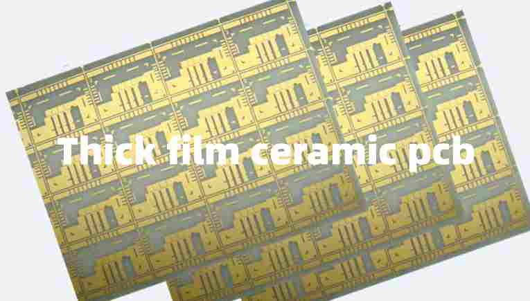
Where ceramic PCBs are showing great performance for consumer electronics, one of their common types, called thick film ceramic PCBs, is emerging as a huge asset for producers and users. These are important to consider because of their components, like carbon resistors that undergo printing.
We use a special polyamide resin for the development of these resistors. The emergence of thick film technology has proved to be successful in the production of these PCBs.
Plus, it renders them different features to distinguish them from the other types. This tech just maximizes the width of the conductor layer present in these PCBs. Such special PCBs have a comparatively high conductor layer thickness that is the main differentiator between them and others. We also use film ink to develop patterns for these PCBs. After the development of the patterns, we apply the same ink on the substrate and pass them through a firing mechanism that ensures complete curation of the ink during the process. This is how we produce this special thick film ceramic layer for these PCBs.
Parameters of Thick Film Ceramic PCB
- Material: We need to use special materials for the production of PCBs, and for this, alumina and aluminum nitride are considerable. Alumina is more common because it is electrically more conductive as compared to others.
- Thickness: The thickness varies as per the requirements of the projects. Some PCBs don’t require extra thick layers, while others do. Therefore producers need to determine the appropriate thickness to avoid complications.
- Dielectric Constant: It is important to remember that dielectric constant values are different for alumina and aluminum nitride. Due to this reason, it is beneficial to use suitable materials when it comes to the development of such PCBs. The dielectric constant means how insulative the material is. Producers pay close attention to this factor before proceeding with the actual production.
- Thermal Conductivity: Both alumina and aluminum nitride have different ranges of thermal conductivity. This factor means how much heat the material can easily let through. For alumina, it is up to 25W/Km, and for aluminum nitride, it is 200W/Km.
- Electrical Resistivity: This is another important factor, and for both materials, it is different. Electrical resistivity means how much current the PCB can stop from flowing.
- Surface Finish: The purpose of surface finish is to keep the resistance as lower as possible so that it can maintain the overall current flow through the system easily. Different conductors and types of surface finish come together to render several benefits to these PCBs.
Benefits of Thick Film Ceramic PCB
- High Thermal Conductivity: When it comes to ceramic PCBs and their sub-categories, impressive thermal conductivity is obvious. Due to this reason, nothing can compare to their heat dissipation ability as well. All of this leads such PCBs to prove to be good regulators of heat on all counts.
- High power handling capacity: No current and power functions can damage these PCBs because they are suitable for such applications that use excessive power all the time. It is because of tensile strength and impressive thermal attributes.
- Miniaturization and high-density packaging: These are supportive of the concept of miniaturization, and due to this reason, these can be developed into highly small sizes. The dielectric layers will be thin, and there will be more space for the arrangement of dense and critical PCB components. This feature is suitable because today, hundreds of electronics follow the technique of miniaturization for great benefits.
- Excellent Electrical Properties: We don’t have to face extreme dielectric loss when we are using these PCBs. The signal disturbance is also less, and due to this reason, intense applications can completely depend on these PCBs.
- Compatibility with high-temperature environments: The ultimate purpose of thick film in these PCBs is to make them endure extreme temperatures easily without damage. Their structure also remains intact, and they keep regulating the heat to protect their critical parts at the same time. Due to this reason, industries like defense, military, and aerospace are relying on these PCBs today.
- Chemical corrosion and resistance: Another great advantage of these PCBs is that you don’t struggle with the fear of corrosion eating up your PCBs. The thick ceramic film eventually fully protects the PCBs from such damage.
- Enhanced reliability and longevity: These PCBs are also more likely to serve you longer because of their dependable electrical and chemical properties. Therefore you can keep taking advantage of their attributes in the long run.
The role of the producers in the development of this layer is important. It is because the finer will be this layer, the better will be the performance of these PCBs. Therefore, in this last section, we are going to explain how the development of a thick ceramic layer takes place on a commercial scale.
How to Reach Thick Film Ceramic PCB?
The only thing that makes these PCBs attractive and sets them apart from the rest is their thick ceramic film. Without this component, unfortunately, PCBs cannot work at their finest. Therefore, producers need to pay close attention to the development of this fine film to make the PCBs seamlessly work. We have to be careful with the development of this film because negligence can ruin the final appearance of the film, and it cannot perform its job as desired as well.
So the first thing we need to do is to place the ceramic, glass, and small metallic fragments in the form of a fine mixture on the substrate. Before this step, it is crucial to check if the substrate is clean or not. The reason is that if any debris and remnants remain on the substrate, these can cause blisters that can eventually compromise the functioning of PCBs.
After the application, we need to pass the PCB through a firing mechanism that takes place at extreme temperatures.
The role of this firing system is to blend the ink with the ceramic mixture completely. It then develops into a thick protective layer on the substrate. Not to forget about the process control measurements important for this process. Once the development procedure is finished, we can proceed with the soldering, PCB component mounting, and layer inspection, in the end, to ensure that the layer is functional or not.


Leave a Reply