Introduction to LPI Soldermask Application
Liquid Photo Imageable (LPI) soldermask is a crucial component in the manufacturing of printed circuit boards (PCBs). It serves as a protective layer that covers the copper traces on the PCB, leaving only the desired areas exposed for soldering components. The application of LPI soldermask is a critical process that directly impacts the quality, reliability, and functionality of the final PCB product. Among the various methods used for applying LPI soldermask, silk screen printing stands out as the most common and widely adopted technique in the industry.
What is LPI Soldermask?
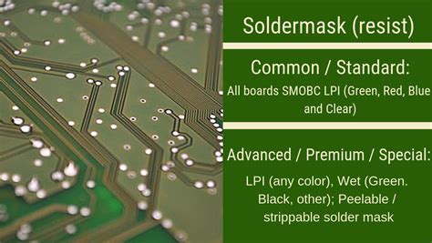
LPI soldermask is a photosensitive polymer coating that is applied to the surface of a PCB. It is designed to protect the copper traces from oxidation, prevent solder bridging, and provide electrical insulation between conductive paths. LPI soldermask is available in various colors, with green being the most popular choice due to its high contrast against the copper traces, making it easier for automated optical inspection (AOI) systems to detect any defects.
Importance of LPI Soldermask Application
The application of LPI soldermask is a vital step in the PCB manufacturing process. A properly applied soldermask ensures:
-
Protection: The soldermask shields the copper traces from environmental factors such as moisture, dust, and mechanical damage, extending the lifespan of the PCB.
-
Insulation: By covering the non-solderable areas, the soldermask prevents short circuits and unintended electrical connections between adjacent traces.
-
Solderability: The soldermask defines the exposed areas where solder can be applied, enabling precise and reliable soldering of components to the PCB.
-
Aesthetics: A well-applied soldermask enhances the visual appeal of the PCB, giving it a professional and finished look.
Silk Screen Printing: The Most Common LPI Soldermask Application Method
Silk screen printing, also known as serigraphy, is the most widely used method for applying LPI soldermask in the PCB industry. This technique involves using a fine mesh screen to transfer the soldermask onto the PCB surface. The screen is made of a stretched mesh fabric, typically polyester or stainless steel, with a stencil of the desired soldermask pattern.
Advantages of Silk Screen Printing
Silk screen printing offers several advantages that make it the preferred choice for LPI soldermask application:
-
Cost-effectiveness: Silk screen printing is a relatively inexpensive method compared to other soldermask application techniques. It requires minimal setup costs and can be easily adapted to different PCB designs and volumes.
-
High throughput: The silk screen printing process is fast and efficient, allowing for high-volume production of PCBs. It can handle multiple boards simultaneously, reducing the overall manufacturing time.
-
Consistency: With proper screen preparation and process control, silk screen printing delivers consistent and uniform soldermask coatings across multiple PCBs. This consistency is crucial for maintaining the quality and reliability of the final product.
-
Flexibility: Silk screen printing can accommodate a wide range of PCB sizes, shapes, and thicknesses. It is suitable for both single-sided and double-sided PCBs, as well as multilayer boards.
The Silk Screen Printing Process
The silk screen printing process for LPI soldermask application involves the following steps:
-
Screen Preparation: A fine mesh screen is coated with a light-sensitive emulsion. The desired soldermask pattern is then exposed onto the emulsion using a photographic process, hardening the exposed areas while leaving the unexposed areas soluble.
-
Soldermask Application: The prepared screen is placed over the PCB, and the LPI soldermask is applied using a squeegee. The squeegee forces the soldermask through the open areas of the screen, depositing it onto the PCB surface.
-
Drying and Curing: After the soldermask is applied, the PCB undergoes a drying process to remove any excess solvents. This is followed by a curing step, where the soldermask is exposed to UV light, causing it to harden and adhere firmly to the PCB surface.
-
Inspection and Touch-up: The PCB is inspected for any defects or irregularities in the soldermask coating. If necessary, touch-up work is performed to correct any issues before proceeding to the next stage of the manufacturing process.
Factors Affecting Silk Screen Printing Quality
To ensure the best results when using silk screen printing for LPI soldermask application, several factors must be considered:
-
Screen Mesh: The mesh count and thread diameter of the screen determine the resolution and thickness of the soldermask coating. Higher mesh counts produce finer details and thinner coatings, while lower mesh counts result in thicker coatings and less detail.
-
Emulsion Thickness: The thickness of the emulsion on the screen affects the amount of soldermask deposited onto the PCB. A thicker emulsion allows for a greater volume of soldermask to be transferred, resulting in a thicker coating.
-
Squeegee Pressure and Angle: The pressure and angle at which the squeegee is applied influence the uniformity and thickness of the soldermask coating. Consistent pressure and a proper angle are essential for achieving an even distribution of the soldermask.
-
Soldermask Viscosity: The viscosity of the LPI soldermask must be carefully controlled to ensure proper flow through the screen and onto the PCB surface. A soldermask with the correct viscosity will result in a smooth, uniform coating without any drips or runs.
-
Curing Conditions: The curing process, including UV exposure time and intensity, must be optimized to ensure complete polymerization of the soldermask. Inadequate curing can lead to poor adhesion, while over-curing may cause brittleness or discoloration of the soldermask.

Comparison with Other LPI Soldermask Application Methods
While silk screen printing is the most common method for applying LPI soldermask, there are other techniques available, each with its own advantages and disadvantages.
Curtain Coating
Curtain coating involves creating a continuous curtain of soldermask that falls onto the moving PCB. This method is suitable for high-volume production and can produce very thin, uniform coatings. However, it requires specialized equipment and may not be cost-effective for smaller production runs.
Spray Coating
Spray coating uses a spray gun to atomize the soldermask and deposit it onto the PCB surface. This method is more flexible than curtain coating and can accommodate a wider range of PCB shapes and sizes. However, it may result in a less uniform coating compared to silk screen printing and curtain coating.
Roller Coating
Roller coating employs a series of rollers to apply the soldermask onto the PCB. This method is fast and can handle large PCB panels, but it may not provide the same level of detail and resolution as silk screen printing.
| Method | Advantages | Disadvantages |
|---|---|---|
| Curtain Coating | – High-volume production – Thin, uniform coatings |
– Requires specialized equipment – Not cost-effective for small runs |
| Spray Coating | – Flexibility in PCB shapes and sizes | – Less uniform coating compared to other methods |
| Roller Coating | – Fast process – Can handle large PCB panels |
– Lower detail and resolution compared to silk screen printing |

Frequently Asked Questions (FAQ)
- What is the most common color for LPI soldermask?
-
Green is the most popular color for LPI soldermask due to its high contrast against the copper traces, making it easier for automated optical inspection (AOI) systems to detect any defects.
-
Can silk screen printing be used for both single-sided and double-sided PCBs?
-
Yes, silk screen printing is suitable for applying soldermask on both single-sided and double-sided PCBs, as well as multilayer boards.
-
What factors influence the quality of silk screen printed soldermask?
-
Several factors affect the quality of silk screen printed soldermask, including screen mesh count, emulsion thickness, squeegee pressure and angle, soldermask viscosity, and curing conditions.
-
Is silk screen printing a cost-effective method for applying LPI soldermask?
-
Yes, silk screen printing is a relatively inexpensive method compared to other soldermask application techniques. It requires minimal setup costs and can be easily adapted to different PCB designs and volumes.
-
What are the advantages of using LPI soldermask on PCBs?
- LPI soldermask provides protection for the copper traces, electrical insulation between conductive paths, improved solderability, and enhanced aesthetics for the PCB.

Conclusion
Silk screen printing is the most common and widely adopted method for applying LPI soldermask in the PCB manufacturing industry. This technique offers several advantages, including cost-effectiveness, high throughput, consistency, and flexibility. By understanding the silk screen printing process and the factors that influence the quality of the soldermask coating, PCB manufacturers can ensure the production of high-quality, reliable, and visually appealing PCBs.
As the demand for advanced and miniaturized electronic devices continues to grow, the importance of LPI soldermask application cannot be overstated. By leveraging the benefits of silk screen printing and continuously optimizing the process, PCB manufacturers can meet the evolving needs of their customers while maintaining a competitive edge in the market.


Leave a Reply