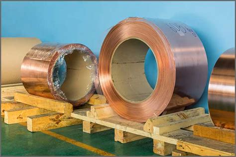
What is PCB Copper Thickness?
PCB copper thickness, also known as copper weight or copper foil thickness, is the thickness of the copper layer that is laminated onto the insulating substrate material of a PCB. The copper thickness is typically measured in ounces per square foot (oz/ft²) or microns (µm).
The most common way to express PCB copper thickness is in ounces per square foot. One ounce of copper per square foot is equivalent to a thickness of approximately 35 microns or 1.4 mils (thousandths of an inch). The following table shows the conversion between ounces per square foot and microns:
| Copper Thickness (oz/ft²) | Copper Thickness (µm) |
|---|---|
| 0.5 oz/ft² | 17.5 µm |
| 1 oz/ft² | 35 µm |
| 2 oz/ft² | 70 µm |
| 3 oz/ft² | 105 µm |
| 4 oz/ft² | 140 µm |
Factors Influencing the Choice of PCB Copper Thickness
Several factors influence the choice of PCB copper thickness, including:
Current Carrying Capacity
One of the primary factors that determine the choice of copper thickness is the current carrying capacity of the PCB. The current carrying capacity refers to the maximum amount of current that can flow through the copper traces without causing damage or excessive heating.
The current carrying capacity of a PCB is directly proportional to the cross-sectional area of the copper traces. Increasing the copper thickness increases the cross-sectional area, allowing the traces to carry more current without overheating. The following table shows the relationship between copper thickness and current carrying capacity:
| Copper Thickness (oz/ft²) | Current Carrying Capacity (Amps/inch) |
|---|---|
| 0.5 oz/ft² | 0.5 A/in |
| 1 oz/ft² | 1.0 A/in |
| 2 oz/ft² | 2.0 A/in |
| 3 oz/ft² | 3.0 A/in |
| 4 oz/ft² | 4.0 A/in |
Signal Integrity
Another factor that influences the choice of copper thickness is signal integrity. Signal integrity refers to the ability of the PCB to maintain the quality and integrity of the electrical signals as they propagate through the copper traces.
Thicker copper traces have lower resistance and lower inductance, which can help to reduce signal distortion and improve signal integrity. However, thicker copper traces also have higher capacitance, which can cause signal reflections and degrade signal quality at high frequencies.
The choice of copper thickness for signal integrity depends on the specific application and the frequency of the signals being carried. For high-speed digital circuits, thinner copper traces may be preferred to minimize capacitance and improve signal quality.
Manufacturing Constraints
The choice of PCB copper thickness is also influenced by manufacturing constraints. PCB manufacturers have limitations on the minimum and maximum copper thickness that they can produce reliably and cost-effectively.
The minimum copper thickness that can be reliably manufactured depends on the capabilities of the PCB fabrication process. Most PCB manufacturers can produce copper thicknesses down to 0.5 oz/ft² (17.5 µm) without significant issues. However, producing thinner copper layers may require specialized manufacturing processes and increase the cost of the PCB.
The maximum copper thickness that can be manufactured is limited by the ability to etch the copper traces accurately and reliably. As the copper thickness increases, it becomes more challenging to etch fine-pitch traces and maintain the required trace width and spacing. Most PCB manufacturers can produce copper thicknesses up to 4 oz/ft² (140 µm) without significant issues.

Most Common PCB Copper Thickness in Manufacturing
The most common PCB copper thickness used in manufacturing depends on the specific application and the requirements of the PCB. However, there are some general guidelines for selecting the appropriate copper thickness based on the current carrying capacity, signal integrity, and manufacturing constraints.
1 oz/ft² (35 µm) Copper Thickness
The most common PCB copper thickness used in manufacturing is 1 oz/ft² (35 µm). This copper thickness provides a good balance between current carrying capacity, signal integrity, and manufacturability.
1 oz/ft² copper thickness is suitable for most general-purpose PCB applications, such as consumer electronics, industrial control systems, and telecommunications equipment. It provides sufficient current carrying capacity for most low to medium power applications, and it can be reliably manufactured by most PCB fabricators.
2 oz/ft² (70 µm) Copper Thickness
For applications that require higher current carrying capacity, such as power electronics and automotive electronics, 2 oz/ft² (70 µm) copper thickness is commonly used. This copper thickness provides twice the current carrying capacity of 1 oz/ft² copper, allowing the PCB to handle higher power levels without overheating.
2 oz/ft² copper thickness is also commonly used in high-frequency applications, such as radio frequency (RF) circuits and microwave circuits. The thicker copper traces help to reduce resistive losses and improve signal quality at high frequencies.
0.5 oz/ft² (17.5 µm) Copper Thickness
For applications that require high-density interconnects and fine-pitch traces, 0.5 oz/ft² (17.5 µm) copper thickness may be used. This copper thickness allows for the fabrication of smaller traces and spaces, enabling higher routing density and smaller PCB sizes.
0.5 oz/ft² copper thickness is commonly used in mobile devices, wearable electronics, and other applications where space is limited, and high-density interconnects are required. However, the thinner copper traces have lower current carrying capacity and may be more susceptible to signal integrity issues.

Impact of PCB Copper Thickness on Performance
The choice of PCB copper thickness can have a significant impact on the performance and reliability of the PCB. Some of the key performance factors that are affected by copper thickness include:
Thermal Management
The copper thickness of a PCB plays a critical role in thermal management. Thicker copper traces have lower thermal resistance and can dissipate heat more effectively than thinner traces. This is particularly important in high-power applications, where the PCB must be able to dissipate the heat generated by the components without overheating.
Increasing the copper thickness can help to improve the thermal performance of the PCB, allowing it to operate at higher power levels without exceeding the maximum operating temperature of the components.
Mechanical Strength
The copper thickness also affects the mechanical strength and durability of the PCB. Thicker copper traces are more robust and less susceptible to mechanical damage, such as cracking or delamination, during handling and assembly.
Increasing the copper thickness can help to improve the mechanical reliability of the PCB, particularly in applications where the PCB is subject to mechanical stress or vibration.
Electromagnetic Interference (EMI)
The copper thickness can also impact the electromagnetic interference (EMI) performance of the PCB. Thicker copper traces have lower resistance and can carry higher currents without generating excessive EMI.
However, thicker copper traces also have higher capacitance, which can cause signal reflections and increase EMI at high frequencies. The choice of copper thickness for EMI performance depends on the specific application and the frequency range of concern.

FAQ
What is the most common PCB copper thickness used in manufacturing?
The most common PCB copper thickness used in manufacturing is 1 oz/ft² (35 µm). This copper thickness provides a good balance between current carrying capacity, signal integrity, and manufacturability for most general-purpose PCB applications.
What factors influence the choice of PCB copper thickness?
The choice of PCB copper thickness is influenced by several factors, including current carrying capacity, signal integrity, and manufacturing constraints. The current carrying capacity of the PCB is directly proportional to the copper thickness, while signal integrity and manufacturability may require thinner or thicker copper traces depending on the specific application.
How does PCB copper thickness affect thermal management?
The copper thickness of a PCB plays a critical role in thermal management. Thicker copper traces have lower thermal resistance and can dissipate heat more effectively than thinner traces. Increasing the copper thickness can help to improve the thermal performance of the PCB, allowing it to operate at higher power levels without overheating.
Can PCB copper thickness affect mechanical strength and durability?
Yes, the copper thickness can affect the mechanical strength and durability of the PCB. Thicker copper traces are more robust and less susceptible to mechanical damage, such as cracking or delamination, during handling and assembly. Increasing the copper thickness can help to improve the mechanical reliability of the PCB.
What is the impact of PCB copper thickness on electromagnetic interference (EMI)?
The copper thickness can impact the electromagnetic interference (EMI) performance of the PCB. Thicker copper traces have lower resistance and can carry higher currents without generating excessive EMI. However, thicker copper traces also have higher capacitance, which can cause signal reflections and increase EMI at high frequencies. The choice of copper thickness for EMI performance depends on the specific application and the frequency range of concern.
Conclusion
Choosing the appropriate PCB copper thickness is essential for ensuring the reliability, performance, and manufacturability of the PCB. The most common PCB copper thickness used in manufacturing is 1 oz/ft² (35 µm), which provides a good balance between current carrying capacity, signal integrity, and manufacturability for most general-purpose applications.
However, the choice of copper thickness depends on several factors, including current carrying capacity, signal integrity, manufacturing constraints, thermal management, mechanical strength, and EMI performance. PCB designers must carefully consider these factors and select the appropriate copper thickness based on the specific requirements of the application.
By understanding the most common PCB copper thickness used in manufacturing and the factors that influence the choice of copper thickness, PCB designers can optimize the performance and reliability of their designs while minimizing manufacturing costs and time to market.


Leave a Reply