What is Plated Through-Hole (PTH) Technology?
Plated Through-Hole (PTH) technology is a critical process in the manufacturing of Printed Circuit Boards (PCBs). It involves creating holes in the PCB substrate and then plating them with a conductive material, typically copper, to establish electrical connections between different layers of the board. This technology has been a cornerstone of PCB Production for decades and continues to play a vital role in modern electronics.
The Process of Creating Plated Through-Holes
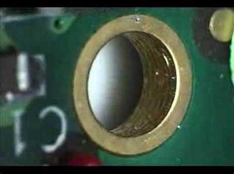
The PTH process begins with drilling holes in the PCB substrate at predetermined locations. These holes are typically drilled using high-speed, computer-controlled drilling machines that ensure precise placement and consistent hole diameters. Once the holes are drilled, the PCB undergoes a series of cleaning and conditioning steps to prepare the surface for the plating process.
The next step is to apply a thin layer of copper to the entire surface of the PCB, including the inside of the drilled holes. This is achieved through a process called electroless copper deposition, which involves immersing the PCB in a chemical bath that contains copper ions. The copper ions adhere to the surface of the PCB and the inside of the holes, creating a thin, uniform layer of copper.
After the electroless copper deposition, the PCB is subjected to an electrolytic plating process. In this process, the PCB is placed in an electrolytic bath containing copper sulfate solution, and an electric current is applied. The electric current causes the copper ions in the solution to migrate towards the PCB and deposit on the surface, including the inside of the holes. This process builds up the thickness of the copper layer, ensuring a robust and reliable electrical connection.
Advantages of Plated Through-Hole Technology
PTH technology offers several key advantages in PCB production:
-
Mechanical Strength: PTH provides excellent mechanical strength to the PCB Assembly. The plated holes act as anchors, securely holding the components in place and preventing them from becoming loose or detached due to vibration or mechanical stress.
-
Electrical Reliability: The plated holes establish a reliable electrical connection between the different layers of the PCB. This ensures that signals can propagate through the board without interruption or degradation, maintaining the integrity of the electrical circuit.
-
Thermal Management: PTH technology also plays a role in thermal management of the PCB. The plated holes can act as thermal vias, allowing heat to dissipate from the components on the surface of the board to the inner layers or to a heatsink. This helps in preventing overheating and enhances the overall reliability of the electronic device.
-
Compatibility with Through-Hole Components: Despite the increasing popularity of surface-mount technology (SMT), through-hole components are still widely used in certain applications. PTH technology allows for the secure mounting and electrical connection of through-hole components, ensuring compatibility with a wide range of electronic components.
The Evolution of Plated Through-Hole Technology
PTH technology has undergone significant advancements over the years to keep pace with the increasing complexity and miniaturization of electronic devices.
Improvements in Drilling Techniques
One area of improvement has been in the drilling techniques used to create the holes in the PCB substrate. Traditional mechanical drilling methods have been largely replaced by laser drilling, which offers several advantages:
-
Smaller Hole Diameters: Laser drilling enables the creation of much smaller hole diameters compared to mechanical drilling. This is crucial for the production of high-density PCBs with fine pitch components.
-
Improved Accuracy: Laser drilling provides superior accuracy and precision in hole placement. This is essential for maintaining the tight tolerances required in modern PCB designs.
-
Reduced Damage: Laser drilling minimizes the risk of damage to the PCB substrate during the drilling process. This helps in maintaining the structural integrity of the board and reduces the chances of defects.
Advancements in Plating Techniques
The plating techniques used in PTH technology have also seen significant advancements:
-
Copper Filling: In addition to the traditional method of plating the inside of the holes, modern PTH processes often involve completely filling the holes with copper. This provides enhanced mechanical strength and improved electrical conductivity.
-
Direct Metallization: Direct metallization techniques have been developed to eliminate the need for electroless copper deposition. These techniques involve directly depositing copper onto the PCB substrate and the inside of the holes using advanced chemical processes. This streamlines the PTH process and reduces the overall manufacturing time.
High Aspect Ratio Plating
Another significant development in PTH technology is the ability to plate holes with high aspect ratios. The aspect ratio refers to the ratio of the hole depth to its diameter. Plating holes with high aspect ratios is challenging because it becomes increasingly difficult to ensure uniform plating as the hole depth increases.
Advanced plating techniques, such as pulse plating and reverse pulse plating, have been developed to address this challenge. These techniques involve modulating the electric current during the plating process to ensure uniform deposition of copper even in deep holes. This has enabled the production of PCBs with high aspect ratio holes, facilitating the development of more compact and dense electronic devices.

The Future of Plated Through-Hole Technology
Despite the advent of alternative technologies like surface-mount technology (SMT) and blind and buried vias, PTH technology continues to hold a significant place in PCB production. It remains the preferred choice for applications that require high mechanical strength, reliability, and compatibility with through-hole components.
However, the future of PTH technology will be shaped by the evolving demands of the electronics industry. Some of the key trends and challenges that will influence the future of PTH include:
-
Miniaturization: As electronic devices continue to shrink in size, there will be a growing demand for PCBs with smaller hole diameters and higher aspect ratios. This will require further advancements in drilling and plating techniques to accommodate these requirements.
-
High-Frequency Applications: With the increasing prevalence of high-frequency applications, such as 5G communication and high-speed data transfer, the electrical performance of PCBs becomes critical. PTH technology will need to evolve to minimize signal loss and ensure reliable performance at high frequencies.
-
Environmental Considerations: There is a growing emphasis on environmentally friendly manufacturing processes in the electronics industry. The PTH process, which involves the use of chemicals and generates waste, will need to be optimized to minimize its environmental impact. This may involve the development of green plating solutions and recycling techniques.
-
Cost Reduction: As with any manufacturing process, there will be a continuous drive to reduce the cost of PTH technology. This may involve the optimization of the plating process, the use of alternative materials, or the adoption of automated inspection techniques to reduce defects and improve yields.

Frequently Asked Questions (FAQ)
- What is the difference between PTH and SMT?
-
PTH (Plated Through-Hole) and SMT (Surface-Mount Technology) are two different methods of mounting components on a PCB. In PTH, the component leads are inserted into plated holes in the PCB and soldered in place. In SMT, the components are placed directly on the surface of the PCB and soldered using a reflow process.
-
Can PTH and SMT be used together on the same PCB?
-
Yes, it is common for PCBs to incorporate both PTH and SMT components. This allows for the use of a wide range of components and provides flexibility in PCB design. However, the manufacturing process becomes more complex when combining both technologies.
-
What is the minimum hole diameter that can be achieved with PTH technology?
-
The minimum hole diameter achievable with PTH technology depends on various factors, such as the PCB Thickness, aspect ratio, and the capabilities of the drilling and plating equipment. With advanced laser drilling and plating techniques, hole diameters as small as 0.1 mm (4 mil) can be achieved.
-
How does PTH technology affect the cost of PCB production?
-
PTH technology generally adds to the cost of PCB production compared to simpler processes like Single-Sided PCBs or PCBs without through-holes. The additional cost is due to the drilling and plating processes involved. However, the cost impact is justified by the improved reliability, mechanical strength, and functionality provided by PTH.
-
What are the challenges in plating high aspect ratio holes?
- Plating high aspect ratio holes (holes with a high depth-to-diameter ratio) presents several challenges. As the aspect ratio increases, it becomes more difficult to ensure uniform plating throughout the entire depth of the hole. Issues such as poor plating coverage, voids, and non-uniform thickness can arise. Advanced plating techniques like pulse plating and optimization of plating parameters are employed to overcome these challenges.

Conclusion
Plated Through-Hole (PTH) technology has been a fundamental pillar of PCB production for decades, and its importance continues to be recognized in the modern electronics industry. The ability to create reliable electrical connections between layers of a PCB while providing mechanical strength and thermal management has made PTH an indispensable process.
As electronic devices continue to evolve, becoming smaller, more complex, and operating at higher frequencies, PTH technology must keep pace. Advancements in drilling and plating techniques have enabled the production of PCBs with smaller hole diameters, higher aspect ratios, and improved electrical performance.
Looking ahead, the future of PTH technology will be shaped by the demands of the electronics industry. Miniaturization, high-frequency applications, environmental considerations, and cost reduction will be key drivers of innovation. As PCB Manufacturers and technology providers rise to these challenges, PTH technology will continue to play a vital role in enabling the next generation of electronic devices.
In conclusion, the importance of Plated Through-Hole technology in PCB production cannot be overstated. Its proven track record of reliability, versatility, and robustness makes it an essential process for a wide range of applications. As the electronics industry continues to push the boundaries of innovation, PTH technology will undoubtedly evolve to meet the demands of the future.
| Aspect | PTH Technology | SMT Technology |
|---|---|---|
| Component Mounting | Components are inserted into plated holes and soldered | Components are placed directly on the PCB surface and soldered |
| Mechanical Strength | Provides excellent mechanical strength due to plated holes acting as anchors | Relies on solder joint strength, generally less mechanically robust |
| Hole Diameters | Typically larger hole diameters compared to SMT pads | Not applicable, uses surface-mount pads |
| PCB Density | Generally lower component density compared to SMT | Allows for higher component density and smaller PCB sizes |
| Manufacturing Process | Involves drilling, plating, and soldering processes | Involves solder paste application, component placement, and reflow soldering |
| Cost | Generally higher cost due to additional drilling and plating processes | Generally lower cost for high-volume production |
Table 1: Comparison of PTH and SMT technologies


Leave a Reply