What is Soldermask Expansion?
Soldermask expansion, also known as solder resist expansion or solder mask pullback, refers to the amount by which the solder mask opening on a printed circuit board (PCB) is enlarged beyond the copper pad dimensions. In other words, it is the value applied to surface mount device (SMD) pads to create a gap between the copper pad and solder mask.
Soldermask is a thin polymer coating applied to the copper traces of a PCB, leaving only the pads, holes, and vias exposed. Its primary function is to prevent solder bridges from forming between closely spaced pads during the soldering process. By expanding the solder mask opening slightly larger than the copper pad, it helps ensure proper solder joint formation and prevents solder from spreading onto adjacent pads or traces.
Importance of Soldermask Expansion
Soldermask expansion plays a crucial role in the manufacturing process of PCBs, particularly for surface mount technology (SMT). Here are some key reasons why soldermask expansion is important:
-
Facilitates Soldering: An appropriate amount of soldermask expansion allows the molten solder to flow onto the exposed copper pad and form a reliable solder joint. If the solder mask opening is too small, it can hinder solder flow and lead to poor or incomplete solder joint formation.
-
Prevents Solder Bridging: Soldermask expansion helps maintain a sufficient gap between adjacent pads, reducing the risk of solder bridging. Solder bridging occurs when solder inadvertently connects two or more pads, causing short circuits and potentially damaging the components or the entire PCB.
-
Accommodates Component Placement: SMD components have specific tolerances for their placement on the PCB. Soldermask expansion provides some flexibility in component placement by allowing slight misalignments during the pick-and-place process. This is particularly important for high-density boards with tight component spacing.
-
Improves Manufacturing Yield: By ensuring proper solder joint formation and preventing solder bridging, soldermask expansion contributes to higher manufacturing yields. It reduces the occurrence of defects and minimizes the need for rework or scrap, ultimately saving time and cost in the production process.
Determining Soldermask Expansion Values
The amount of soldermask expansion applied to SMD pads depends on various factors, including the PCB design, component package size, and manufacturing capabilities. Here are some considerations when determining soldermask expansion values:
IPC Standards
The IPC (Association Connecting Electronics Industries) provides guidelines for soldermask expansion in their standards, such as IPC-7351 and IPC-SM-782. These standards recommend specific soldermask expansion values based on the component package size and the desired solder joint reliability.
For example, IPC-7351 provides the following recommendations for soldermask expansion:
| Package Size | Minimum Soldermask Expansion |
|---|---|
| 0201 | 0.05 mm (0.002 in) |
| 0402 | 0.10 mm (0.004 in) |
| 0603 | 0.10 mm (0.004 in) |
| 0805 | 0.10 mm (0.004 in) |
| 1206 | 0.15 mm (0.006 in) |
These values serve as a starting point and can be adjusted based on specific design requirements and manufacturing capabilities.
PCB Fabrication Capabilities
The achievable soldermask expansion values also depend on the capabilities of the PCB fabrication facility. Different manufacturers may have varying limitations in terms of minimum soldermask expansion they can reliably produce.
It’s important to communicate with the PCB fabricator and understand their specific capabilities and recommendations for soldermask expansion. They can provide guidance based on their equipment, processes, and experience to ensure the desired soldermask expansion is achievable and consistent.
Design Considerations
When determining soldermask expansion values, designers should consider the following factors:
-
Component Density: In high-density designs with closely spaced components, smaller soldermask expansion values may be necessary to avoid solder bridging. However, this should be balanced with the need for adequate solder joint formation.
-
Pad Size and Shape: The size and shape of the SMD pads can influence the soldermask expansion value. Larger pads or irregular shapes may require greater expansion to ensure proper solder coverage and prevent solder mask from encroaching onto the pad surface.
-
Solder Paste Stencil Design: The soldermask expansion should be coordinated with the solder paste stencil aperture design. The stencil aperture should be slightly smaller than the soldermask opening to prevent solder paste from spreading beyond the pad area during the printing process.
-
Manufacturing Process: The soldermask expansion value may need to be adjusted based on the specific manufacturing processes used, such as solder paste printing, component placement, and reflow soldering. Different processes may have different tolerances and requirements for soldermask expansion.

Applying Soldermask Expansion in PCB Design Software
Most PCB design software tools provide options to define and apply soldermask expansion values to SMD pads. The exact steps may vary depending on the specific software being used, but the general process is as follows:
-
Define Soldermask Expansion Rules: In the PCB design software, create soldermask expansion rules based on the desired values for different component packages or pad sizes. These rules can be defined globally or assigned to specific components or pad shapes.
-
Assign Soldermask Expansion to Pads: Select the SMD pads or components and assign the appropriate soldermask expansion rule to them. This can be done individually or in groups, depending on the design requirements.
-
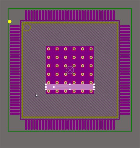
Verify Soldermask Expansion: After applying the soldermask expansion rules, visually inspect the PCB layout to ensure the solder mask openings are correctly expanded around the pads. Use the software’s measurement tools to verify the expansion values meet the desired specifications.
-
Generate Manufacturing Files: When generating the manufacturing files for PCB fabrication, ensure that the soldermask expansion settings are included in the output files, such as Gerber files or ODB++ files. This information is critical for the PCB manufacturer to accurately create the soldermask layer.
It’s important to consult the documentation or support resources of the specific PCB design software being used for detailed instructions on applying soldermask expansion.

Soldermask Expansion and PCB Assembly
Soldermask expansion not only affects the PCB fabrication process but also plays a role in the subsequent PCB assembly stage. Here’s how soldermask expansion influences PCB assembly:
Solder Paste Printing
During the solder paste printing process, a stencil is used to apply solder paste onto the SMD pads. The stencil apertures are typically designed to be slightly smaller than the soldermask openings to prevent solder paste from spreading beyond the pad area.
If the soldermask expansion is too small, it can lead to insufficient solder paste coverage on the pads, resulting in weak or incomplete solder joints. On the other hand, excessive soldermask expansion can cause solder paste to spread onto adjacent pads or traces, increasing the risk of solder bridging.
Component Placement
Soldermask expansion provides some tolerance for component placement during the pick-and-place process. The expanded soldermask opening allows for slight misalignments of components while still ensuring proper solder joint formation.
However, if the soldermask expansion is insufficient, it can make component placement more challenging, especially for small or fine-pitch components. Misaligned components may not have adequate contact with the solder paste, leading to poor solder joints or component tilting.
Reflow Soldering
During the reflow soldering process, the PCB is subjected to a controlled temperature profile to melt the solder paste and form solder joints between the components and pads. Soldermask expansion plays a role in the formation and reliability of these solder joints.
Appropriate soldermask expansion allows the molten solder to flow onto the exposed copper pad and form a robust solder joint. It also helps prevent solder from spreading onto adjacent pads or traces, reducing the risk of short circuits or solder bridges.
If the soldermask expansion is insufficient, it can hinder solder flow and lead to incomplete or weak solder joints. Conversely, excessive expansion may cause solder to spread too much, potentially causing solder bridging or affecting the mechanical strength of the solder joint.

FAQ
1. What is the purpose of soldermask expansion?
Soldermask expansion serves to create a gap between the copper pad and the solder mask on a PCB. It helps facilitate proper solder joint formation, prevents solder bridging, accommodates component placement tolerances, and improves overall manufacturing yield.
2. How is soldermask expansion typically specified?
Soldermask expansion is typically specified as a minimum value, measured in millimeters or inches. It represents the additional amount by which the solder mask opening is enlarged beyond the copper pad dimensions. The specific value depends on factors such as the component package size, PCB design, and manufacturing capabilities.
3. What are the consequences of insufficient soldermask expansion?
Insufficient soldermask expansion can lead to several issues, including:
– Difficulty in achieving proper solder joint formation due to limited solder flow onto the pads.
– Increased risk of solder bridging between adjacent pads or traces.
– Challenges in component placement, especially for small or fine-pitch components.
– Potential for incomplete or weak solder joints, affecting the reliability of the PCB assembly.
4. Can soldermask expansion be too large?
Yes, excessive soldermask expansion can also cause problems. If the soldermask opening is too large, it may allow solder to spread beyond the intended pad area, potentially causing solder bridging or affecting the mechanical strength of the solder joint. It’s important to strike a balance and specify an appropriate soldermask expansion value based on the specific design requirements and manufacturing capabilities.
5. How can I ensure the correct soldermask expansion is applied in my PCB design?
To ensure the correct soldermask expansion is applied in your PCB design, follow these steps:
1. Consult the relevant IPC standards and guidelines for recommended soldermask expansion values based on component package sizes.
2. Communicate with your PCB fabrication partner to understand their specific capabilities and recommendations for soldermask expansion.
3. Define soldermask expansion rules in your PCB design software based on the desired values for different component packages or pad sizes.
4. Assign the appropriate soldermask expansion rules to the SMD pads or components in your PCB layout.
5. Verify the soldermask expansion values through visual inspection and measurements in the PCB design software.
6. Ensure the soldermask expansion settings are included in the manufacturing files generated for PCB fabrication.
By following these steps and considering the specific requirements of your PCB design and manufacturing process, you can effectively apply soldermask expansion to ensure reliable solder joint formation and successful PCB assembly.


Leave a Reply