Introduction to Solder Mask
Solder mask, also known as solder resist or solder stop, is a crucial component in the manufacturing of printed circuit boards (PCBs). It is a thin, protective layer applied to the copper traces and pads on a PCB, leaving only the areas that need to be soldered exposed. The primary purpose of the solder mask is to prevent accidental short circuits and protect the copper traces from oxidation and environmental damage.
Functions of Solder Mask
-
Insulation: Solder mask acts as an insulating layer, preventing accidental contact between adjacent copper traces and components, thus avoiding short circuits.
-
Protection: The solder mask protects the copper traces from oxidation, corrosion, and other environmental factors that could degrade the performance of the PCB over time.
-
Solder Control: By selectively exposing only the areas that need to be soldered, the solder mask helps control the flow of solder during the assembly process, ensuring precise and reliable solder joints.
-
Aesthetics: Solder mask is available in various colors, with green being the most common. The color of the solder mask can enhance the visual appeal of the PCB and make it easier to inspect for defects.
Composition and Application of Solder Mask
Materials Used in Solder Mask
Solder mask is typically composed of a polymer-based ink or paint, which is applied to the PCB surface. The most common types of solder mask materials include:
-
Liquid Photoimageable Solder Mask (LPSM): LPSM is a photosensitive polymer that is applied as a liquid and then exposed to UV light through a photomask to create the desired pattern.
-
Dry Film Photoimageable Solder Mask (DFSM): DFSM is a photosensitive film that is laminated onto the PCB surface and then exposed to UV light through a photomask to create the desired pattern.
-
Epoxy Liquid Solder Mask: This type of solder mask is a two-part epoxy that is screen printed onto the PCB surface and then cured using heat.
Application Methods
The application of solder mask involves several steps:
-
Cleaning: The PCB surface is thoroughly cleaned to remove any contaminants that could affect the adhesion of the solder mask.
-
Application: The solder mask material is applied to the PCB surface using one of the following methods:
- Screen Printing: Used for epoxy liquid solder mask, the material is forced through a mesh screen onto the PCB surface.
- Curtain Coating: Used for LPSM, the liquid solder mask is poured onto the PCB surface and then spread evenly using a coating blade.
-
Lamination: Used for DFSM, the film is laminated onto the PCB surface using heat and pressure.
-
Exposure: For photoimageable solder masks (LPSM and DFSM), the PCB is exposed to UV light through a photomask, which selectively hardens the solder mask in the desired areas.
-
Developing: After exposure, the unexposed areas of the photoimageable solder mask are removed using a chemical developer, leaving only the hardened solder mask on the PCB surface.
-
Curing: The solder mask is then cured using heat to ensure proper adhesion and durability.

Properties and Performance of Solder Mask
Electrical Properties
Solder mask plays a critical role in maintaining the electrical integrity of a PCB. Some of the key electrical properties of solder mask include:
-
Dielectric Strength: Solder mask must have a high dielectric strength to prevent electrical breakdown between adjacent copper traces and components.
-
Insulation Resistance: The solder mask should provide high insulation resistance to minimize leakage currents and maintain signal integrity.
-
Dielectric Constant: A low dielectric constant is desirable for high-frequency applications to minimize signal loss and distortion.
Mechanical Properties
The mechanical properties of solder mask are essential for ensuring the longevity and reliability of the PCB. Some of the key mechanical properties include:
-
Adhesion: Solder mask must have excellent adhesion to the copper traces and the PCB substrate to prevent delamination and maintain the integrity of the protective layer.
-
Flexibility: The solder mask should be flexible enough to withstand the thermal and mechanical stresses encountered during the assembly process and the PCB’s operational life.
-
Hardness: A certain degree of hardness is required to prevent damage to the solder mask during handling and assembly.
Chemical Resistance
Solder mask must be resistant to various chemicals encountered during the PCB manufacturing process and its operational life. Some of the key chemical resistance properties include:
-
Resistance to Solvents: Solder mask should be resistant to common solvents used in PCB Cleaning and processing, such as isopropyl alcohol and acetone.
-
Resistance to Acids and Bases: The solder mask must withstand exposure to mild acids and bases used in the PCB manufacturing process, such as fluxes and cleaning agents.
-
Resistance to Moisture: Solder mask should provide a barrier against moisture to prevent corrosion of the copper traces and other components.
Thermal Properties
PCBs are often subjected to high temperatures during the assembly process and operation. Solder mask must be able to withstand these thermal stresses without degradation. Some of the key thermal properties include:
-
Glass Transition Temperature (Tg): The Tg of the solder mask should be high enough to prevent softening or deformation during the soldering process and operation.
-
Coefficient of Thermal Expansion (CTE): The CTE of the solder mask should be compatible with that of the PCB substrate and components to minimize stress and warpage during thermal cycling.
-
Thermal Decomposition: Solder mask must have a high decomposition temperature to prevent degradation during the soldering process and operation.

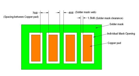
Solder Mask Design Considerations
Solder Mask Clearance
Solder mask clearance refers to the distance between the edge of the exposed copper pad and the edge of the solder mask opening. Proper solder mask clearance is essential for ensuring reliable solder joints and preventing solder bridges. The clearance requirements depend on various factors, such as the PCB manufacturing process, component sizes, and soldering method.
Some common solder mask clearance guidelines include:
| Pad Size | Minimum Clearance |
|---|---|
| < 0.5 mm | 0.05 mm |
| 0.5 – 1.0 mm | 0.1 mm |
| 1.0 – 2.0 mm | 0.15 mm |
| > 2.0 mm | 0.2 mm |
Solder Mask Sliver
Solder mask sliver refers to the narrow strip of solder mask between two adjacent copper pads or traces. Insufficient solder mask sliver can lead to solder bridging and short circuits. The minimum solder mask sliver width depends on the PCB manufacturing process and the solder mask material used.
Some common solder mask sliver guidelines include:
| Solder Mask Type | Minimum Sliver Width |
|---|---|
| LPSM | 0.1 mm |
| DFSM | 0.15 mm |
| Epoxy Liquid | 0.2 mm |
Solder Mask Thickness
The thickness of the solder mask affects its insulation properties, durability, and the overall quality of the PCB. The optimal solder mask thickness depends on the specific application and the solder mask material used. Some common solder mask thickness ranges include:
| Solder Mask Type | Thickness Range |
|---|---|
| LPSM | 12 – 25 µm |
| DFSM | 15 – 30 µm |
| Epoxy Liquid | 20 – 40 µm |
Solder Mask Color
The color of the solder mask is primarily chosen for aesthetic reasons, but it can also serve functional purposes. Some common solder mask colors and their applications include:
-
Green: The most common color, green solder mask provides good contrast for inspection and is suitable for most applications.
-
Blue: Often used in high-reliability applications, such as aerospace and military, due to its high resistance to UV light and humidity.
-
Red: Sometimes used in high-voltage applications to provide a visual warning of potential electrical hazards.
-
Black: Used in applications where light sensitivity is a concern, such as optical sensors and displays.
-
White: Can be used to enhance the visibility of silk-screened text and markings on the PCB surface.

Solder Mask Defects and Quality Control
Common Solder Mask Defects
Several defects can occur during the solder mask application process, which can affect the performance and reliability of the PCB. Some common solder mask defects include:
-
Pinholes: Small holes in the solder mask that expose the underlying copper, increasing the risk of short circuits and corrosion.
-
Solder Mask Bridges: Unintended connections between adjacent solder mask openings, which can lead to solder bridging during assembly.
-
Solder Mask Residue: Incomplete removal of the solder mask in exposed areas, which can interfere with soldering and component placement.
-
Solder Mask Delamination: Separation of the solder mask from the PCB surface, which can expose the copper traces to damage and environmental factors.
-
Solder Mask Cracking: Fractures in the solder mask caused by thermal or mechanical stress, which can compromise the protection of the copper traces.
Quality Control Methods
To ensure the quality and consistency of the solder mask application, several quality control methods are employed:
-
Visual Inspection: PCBs are visually inspected for defects such as pinholes, bridges, residue, and delamination.
-
Microscopic Inspection: High-magnification microscopes are used to detect smaller defects and measure solder mask clearance and sliver widths.
-
Thickness Measurement: The thickness of the solder mask is measured using specialized equipment, such as a micrometer or a coating thickness gauge.
-
Adhesion Testing: The adhesion of the solder mask to the PCB surface is tested using methods such as the cross-hatch test or the tape test.
-
Electrical Testing: PCBs are subjected to electrical tests, such as insulation resistance and dielectric withstanding voltage, to ensure the integrity of the solder mask.
Frequently Asked Questions (FAQ)
- What is the purpose of solder mask on a PCB?
-
Solder mask serves as a protective layer for the copper traces on a PCB, preventing short circuits, oxidation, and environmental damage. It also helps control the flow of solder during the assembly process.
-
What are the most common solder mask materials?
-
The most common solder mask materials are Liquid Photoimageable Solder Mask (LPSM), Dry Film Photoimageable Solder Mask (DFSM), and Epoxy Liquid Solder Mask.
-
What factors determine the solder mask clearance and sliver width?
-
Solder mask clearance and sliver width depend on factors such as the PCB manufacturing process, component sizes, soldering method, and the specific solder mask material used.
-
How does the color of the solder mask affect the PCB’s functionality?
-
The color of the solder mask is primarily chosen for aesthetic reasons, but certain colors can serve functional purposes, such as blue for high-reliability applications or black for light-sensitive applications.
-
What are some common quality control methods used for solder mask application?
- Common quality control methods for solder mask application include visual inspection, microscopic inspection, thickness measurement, adhesion testing, and electrical testing.
Conclusion
Solder mask is a vital component in the manufacturing of printed circuit boards, providing essential protection for the copper traces and ensuring the reliability and longevity of the PCB. By understanding the composition, application methods, properties, and design considerations of solder mask, PCB designers and manufacturers can create high-quality, robust PCBs that meet the demands of various applications.
As PCB technology continues to evolve, so too will the materials and processes used in solder mask application. Advancements in solder mask formulations and application methods will enable the production of even more reliable, compact, and high-performance PCBs, driving innovation across numerous industries, from consumer electronics to aerospace and beyond.


Leave a Reply