What is SMT?
SMT stands for Surface Mount Technology. It is a method for constructing electronic circuits in which the components are mounted directly onto the surface of printed circuit boards (PCBs). SMT has largely replaced the through-hole technology construction method of fitting components with wire leads into holes in the circuit board.
In the industry, SMT has become the standard way of manufacturing PCBs for several reasons:
- Components are getting smaller and more compact
- High component density allows for smaller PCBs and devices
- Suitable for high-volume, automated production
- Lower initial cost and faster assembly
- Fewer holes need to be drilled through PCBs
- Both sides of the PCB can be used for component placement
The SMT component placement process is highly automated using pick-and-place machines. A typical SMT assembly line has 3 main steps:
-
Solder Paste Application – Solder paste (a sticky mixture of powdered solder and flux) is applied to the PCB pads using a stencil or screen printer.
-
Component Placement – The SMT components are placed on the PCB at their designated locations. High-speed pick-and-place machines rapidly place hundreds of small components.
-
Reflow Soldering – The PCB passes through an oven that heats the board to a temperature where the solder paste melts. The components are soldered to the PCB pads as the solder cools and solidifies.
After these main steps, the assembled PCBs typically go through inspection, testing, and cleaning before final packaging and shipment.
What is SMD?
SMD stands for Surface Mounted Device. This refers to the small electronic components that are made specifically for use in surface mount technology (SMT) assembly. SMD components are attached directly to the surface of a printed circuit board (PCB), rather than being inserted through holes like through-hole components.
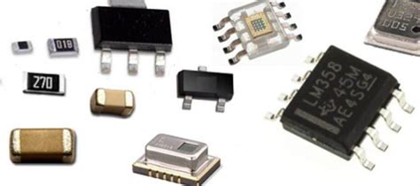
SMDs come in a variety of sizes and packages designed for compatibility with automated SMT assembly equipment. Common SMD Packages include:
- Resistors and capacitors: 0201, 0402, 0603, 0805, 1206, etc.
- Transistors and diodes: SOT-23, SC-70, etc.
- Integrated circuits: SOIC, TSOP, QFP, BGA, etc.
The size of an SMD is usually indicated by a 4-digit number, e.g. 0805, where:
– The first two digits represent the length of the component in hundredths of an inch
– The second two digits represent the width in hundredths of an inch
So an 0805 SMD measures approximately 0.08 inches long by 0.05 inches wide.
Compared to through-hole components, SMDs offer several advantages:
- Smaller size allows for higher component density on the PCB
- Lower cost in high-volume production
- Faster automated assembly
- Shorter pins produce better high-frequency performance
- Smaller packages have lower parasitic inductance and capacitance
The main tradeoff is that SMDs are more difficult to manually solder and replace. Through-hole mounting provides stronger mechanical bonds than SMDs. But in most modern applications, the benefits of SMDs outweigh the drawbacks.

SMT vs SMD: What’s the Difference?
While SMT and SMD are closely related terms, they refer to different things. It’s important to understand the distinction:
- SMT (surface mount technology) refers to the method and process of mounting components onto PCBs
- SMD (surface mounted device) refers to the actual components that are designed for the SMT process
In other words, SMT is the technique and SMD is the component. You wouldn’t say “SMT components” or “SMD soldering” – instead, you solder SMD components using SMT assembly techniques.
Here’s a comparison table to summarize the key differences:
| SMT | SMD |
|---|---|
| PCB Assembly method | Electronic component type |
| Process of soldering components to the PCB surface | Components designed for SMT assembly |
| Involves screen printing, pick-and-place machines, reflow ovens | Available in various package sizes like 0402, 0603, SOIC, QFP |
| Enables high-speed, high-volume, low-cost production | Offers small size, low cost, high performance vs through-hole |

Advantages of SMT and SMD
The widespread adoption of surface mount technology and surface mounted devices has revolutionized PCB design and assembly. Compared to older through-hole techniques, SMT and SMD offer many important benefits:
Smaller Size and Higher Density
The most obvious advantage of SMDs is their compact size compared to equivalent through-hole components. Smaller components allow for much higher densities on the PCB, which enables the design of smaller, lighter, more feature-rich electronics.
Faster and Lower-Cost Assembly
SMT is ideal for automated PCB assembly using high-speed pick-and-place equipment. Through-hole components require more time-consuming and expensive manual insertion and wave soldering. With SMT, production is much faster and the cost per board drops dramatically in high volumes.
Improved Performance
SMDs have shorter pins which produces better high-frequency and RF performance compared to through-hole packages. SMDs also have lower parasitic inductance and capacitance.
Double-Sided PCBs
With through-hole mounting, component leads protrude through the bottom of the board, blocking that space. But SMT allows components to be soldered directly to both sides of the PCB, enabling higher density and more compact designs.

SMT and SMD Best Practices
To get the best results with surface mount PCB assembly, there are some key guidelines and best practices to follow. Careful design and process control helps ensure manufacturing yield and reliability.
SMD Padstack Design
The foundation of a good SMT assembly is proper PCB footprint and padstack design. The arrangement of copper pads on the PCB must exactly match the arrangement of pins or leads on the component. Additionally:
- The pad size should be slightly larger than the component lead, allowing for some placement tolerance
- The pad shape may be rectangular or circular depending on the component
- Include a solder mask opening around the pad to prevent bridging
Stencil Design
Solder paste stencils should be designed to match the pad layout on the PCB. Stencil aperture size and shape determine the amount of solder paste deposited. Guidelines for stencil design include:
- Stencil thickness typically ranges from 0.004″ to 0.008″ (0.1-0.2mm)
- The aperture should be slightly smaller than the pad to allow for paste spread
- Include aperture reduction and gasketing for fine-pitch components
Reflow Profile
The reflow soldering process is critical to forming reliable solder joints. The reflow oven temperature profile must be carefully optimized for the solder paste and components used. Key aspects of the profile include:
- Preheat ramp rate and soak time to activate flux and remove volatiles
- Peak temperature and time above liquidus (TAL) to fully melt solder
- Cool-down ramp rate to control solder joint grain structure
- Reflow in nitrogen (N2) atmosphere to minimize oxidation
Inspection
SMT assemblies should be inspected immediately after soldering to check for defects. Automated optical inspection (AOI) systems are commonly used to check Solder Joint Quality, component placement, and other issues. X-ray inspection may be used for hidden joints like BGAs. Electrical testing verifies proper PCB functionality before shipment.
FAQ
What is the main difference between SMT and SMD?
SMT (surface mount technology) refers to the PCB assembly method, while SMD (surface mounted device) refers to the actual component packages. SMDs are soldered to the board using the SMT process.
Are SMD components better than through-hole?
SMDs offer several advantages over through-hole components:
– Smaller size and lower weight
– Lower cost, especially in high volumes
– Faster automated assembly
– Improved high-frequency performance
However, through-hole still provides stronger physical attachment to the PCB.
What are some common SMD packages?
Common two-terminal SMD packages include:
– 0402: 0.04″ x 0.02″ (1.0mm x 0.5mm)
– 0603: 0.06″ x 0.03″ (1.6mm x 0.8mm)
– 0805: 0.08″ x 0.05″ (2.0mm x 1.25mm)
– 1206: 0.12″ x 0.06″ (3.2mm x 1.6mm)
For ICs, common SMD packages include:
– Small-outline integrated circuit (SOIC)
– Quad flat pack (QFP)
– Ball grid array (BGA)
– Quad flat no-leads (QFN)
What equipment is used for SMT assembly?
A typical SMT assembly line includes:
– Solder paste printer
– Pick-and-place machine
– Reflow soldering oven
– Automated optical inspection (AOI)
How reliable are SMDs compared to through-hole?
When properly designed and assembled, SMDs are very robust and reliable. However, SMDs are more sensitive to thermal expansion issues than through-hole components. And large SMDs like BGAs may be prone to cracking under extreme mechanical stress.


Leave a Reply