What is Through-Hole Soldering?
Through-hole soldering is a method of connecting electronic components to a PCB by inserting the component leads through pre-drilled holes in the board and soldering them to the copper pads on the opposite side. This technique is often used for larger components, such as capacitors, resistors, and connectors, that require a more robust mechanical connection to the PCB.
Advantages of Through-Hole Soldering
- Stronger mechanical connection compared to surface-mount soldering
- Easier to inspect and repair
- Better suited for high-power and high-voltage applications
- More accessible for beginners and hobbyists
Disadvantages of Through-Hole Soldering
- Requires more space on the PCB compared to surface-mount components
- Slower assembly process compared to surface-mount soldering
- Limited component density due to the larger footprint of through-hole components
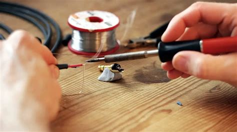
Manual Soldering
Manual soldering is the most common and versatile method for through-hole soldering. It involves using a soldering iron to heat the component lead and the copper pad simultaneously, allowing the solder to flow and create a strong electrical and mechanical connection.
Tools and Materials Required
- Soldering iron with adjustable temperature control
- Soldering iron tip (chisel or conical shape)
- Solder wire (lead-based or lead-free)
- Flux (rosin core or separate flux pen)
- Soldering iron stand
- Sponge or brass wool for cleaning the soldering iron tip
- Tweezers or pliers for handling components
- Wire cutters for trimming component leads
Step-by-Step Guide to Manual Soldering
- Prepare the soldering iron by setting the temperature to the appropriate level for the solder and components being used.
- Clean the soldering iron tip using a damp sponge or brass wool to remove any oxidation or residue.
- Apply a small amount of solder to the tip of the iron to help with heat transfer (this is called tinning the tip).
- Insert the component lead through the designated hole in the PCB, ensuring that it is seated properly.
- Bend the component lead slightly to hold it in place.
- Place the soldering iron tip against the component lead and the copper pad simultaneously.
- Apply solder to the joint, allowing it to flow around the lead and pad. Use just enough solder to create a smooth, shiny joint.
- Remove the soldering iron and allow the joint to cool for a few seconds.
- Trim the excess component lead using wire cutters, leaving approximately 1-2mm of lead above the solder joint.
Tips for Successful Manual Soldering
- Maintain a clean and well-tinned soldering iron tip for optimal heat transfer and joint quality.
- Use the appropriate temperature for the solder and components being used to avoid damaging the components or creating poor joints.
- Apply just enough solder to create a strong, shiny joint. Avoid using too much solder, which can result in bridging between adjacent pads or a messy appearance.
- Work quickly to minimize the heat exposure to the components and PCB, which can cause damage or delamination.
- Practice proper safety procedures, such as using a fume extractor or working in a well-ventilated area to avoid inhaling solder fumes.

Wave Soldering
Wave soldering is an automated process used for soldering through-hole components on a large scale. In this method, the PCB is passed over a molten solder wave, which flows up through the holes and creates a solder joint between the component leads and the copper pads.
Advantages of Wave Soldering
- High-speed, automated process suitable for large-scale production
- Consistent solder joint quality
- Reduced labor costs compared to manual soldering
- Ability to solder multiple components simultaneously
Disadvantages of Wave Soldering
- High initial equipment costs
- Limited flexibility for design changes or small-batch production
- Requires specialized setup and maintenance
- Potential for thermal shock to components due to rapid heating and cooling
Wave Soldering Process
- PCB Preparation: The PCB is designed with through-hole components and a solder mask to protect areas that should not be soldered. A fixture is used to hold the PCB securely during the soldering process.
- Fluxing: The PCB is passed through a fluxing station, where a thin layer of flux is applied to the bottom side of the board to help remove oxides and improve solder wetting.
- Preheating: The PCB is preheated to minimize thermal shock and improve solder flow. This step also activates the flux and evaporates any remaining solvents.
- Solder Wave: The preheated PCB is passed over a molten solder wave, which is typically a mixture of tin, lead, and other metals. The solder flows up through the holes and creates a solder joint between the component leads and the copper pads.
- Cooling: After passing over the solder wave, the PCB is cooled to allow the solder joints to solidify. Cooling can be achieved through natural convection or forced air cooling.
- Cleaning: If necessary, any remaining flux residue is removed from the PCB using a cleaning agent or solvent.

Selective Soldering
Selective soldering is a process that combines the flexibility of manual soldering with the automation of wave soldering. In this method, a specialized machine is used to apply solder to specific areas of the PCB, allowing for the soldering of through-hole components in a targeted manner.
Advantages of Selective Soldering
- Flexibility to solder specific areas or components on a PCB
- Suitable for mixed-technology boards with both through-hole and surface-mount components
- Reduced thermal stress on sensitive components compared to wave soldering
- Improved solder joint quality compared to manual soldering
Disadvantages of Selective Soldering
- Higher equipment costs compared to manual soldering
- Slower process compared to wave soldering for high-volume production
- Requires specialized programming and setup for each PCB design
Selective Soldering Process
- PCB Preparation: The PCB is designed with through-hole components and a solder mask to protect areas that should not be soldered. A fixture is used to hold the PCB securely during the soldering process.
- Fluxing: A small amount of flux is applied to the specific areas or components to be soldered, typically using a precision dispenser or spray nozzle.
- Preheating: The PCB is preheated to minimize thermal shock and improve solder flow. This step also activates the flux and evaporates any remaining solvents.
- Soldering: A specialized soldering nozzle is used to apply molten solder to the targeted areas or components. The nozzle is programmed to move along a specific path, ensuring precise solder application.
- Cooling: After soldering, the PCB is cooled to allow the solder joints to solidify. Cooling can be achieved through natural convection or forced air cooling.
- Inspection: The soldered areas are inspected visually or using automated optical inspection (AOI) to ensure joint quality and detect any defects.

Reflow Soldering
Reflow soldering is a method primarily used for surface-mount components but can also be adapted for through-hole soldering. In this process, solder paste (a mixture of powdered solder and flux) is applied to the PCB pads, and the components are placed on top. The entire assembly is then heated in a reflow oven, melting the solder and creating a strong bond between the components and the PCB.
Advantages of Reflow Soldering for Through-Hole Components
- Ability to solder both surface-mount and through-hole components in a single process
- Consistent solder joint quality
- Reduced thermal stress on components compared to wave soldering
- Suitable for high-volume production
Disadvantages of Reflow Soldering for Through-Hole Components
- Requires specialized equipment and solder paste
- Limited to components that can withstand the reflow temperature profile
- May require additional steps, such as pin-in-paste or intrusive reflow, for through-hole components
Reflow Soldering Process for Through-Hole Components
- PCB Preparation: The PCB is designed with both surface-mount and through-hole components. Solder paste is applied to the pads using a stencil or syringe.
- Component Placement: Surface-mount components are placed on the solder paste using a pick-and-place machine or manual placement. Through-hole components are inserted into the designated holes.
- Pin-in-Paste or Intrusive Reflow: For through-hole components, additional solder paste may be applied to the component leads using a pin-in-paste technique, or the leads may be bent to make contact with the solder paste on the surface of the PCB (intrusive reflow).
- Reflow: The PCB assembly is placed in a reflow oven, which follows a specific temperature profile to melt the solder paste and create a strong bond between the components and the PCB.
- Cooling: After reflow, the PCB is cooled to allow the solder joints to solidify.
- Inspection: The soldered PCB is inspected visually or using automated optical inspection (AOI) to ensure joint quality and detect any defects.
Comparison of Through-Hole Soldering Methods
| Method | Advantages | Disadvantages | Application |
|---|---|---|---|
| Manual Soldering | – Flexibility – Low cost – Suitable for prototyping and small-batch production |
– Time-consuming – Operator skill dependent – Inconsistent joint quality |
– Prototyping – Small-batch production – Rework and repair |
| Wave Soldering | – High-speed – Automated – Consistent joint quality – Suitable for high-volume production |
– High initial equipment costs – Limited flexibility – Potential for thermal shock |
– High-volume production – Simple PCB designs with mostly through-hole components |
| Selective Soldering | – Flexibility – Suitable for mixed-technology boards – Reduced thermal stress – Improved joint quality |
– Higher equipment costs – Slower than wave soldering – Requires specialized programming |
– Mixed-technology boards – Targeted soldering of specific areas or components |
| Reflow Soldering | – Suitable for both surface-mount and through-hole components – Consistent joint quality – Reduced thermal stress – High-volume production |
– Requires specialized equipment and solder paste – Limited to components that can withstand reflow temperatures – May require additional steps for through-hole components |
– High-volume production – Mixed-technology boards with surface-mount and through-hole components |
Frequently Asked Questions (FAQ)
- What is the difference between lead-based and lead-free solder?
-
Lead-based solder contains a mixture of tin and lead, typically in a ratio of 60/40 or 63/37. Lead-free solder, on the other hand, is made from a combination of tin, silver, and copper (SAC alloys) or other lead-free alloys. Lead-free solder has a higher melting point and requires slightly different soldering techniques compared to lead-based solder. The use of lead-free solder has become more common due to environmental and health concerns associated with lead.
-
How do I choose the right soldering iron tip for through-hole soldering?
-
When selecting a soldering iron tip for through-hole soldering, consider the size and shape of the components and pads you will be working with. Chisel tips and conical tips are the most common choices for through-hole soldering. Chisel tips offer a larger contact area, making them suitable for soldering larger components or multiple leads simultaneously. Conical tips provide more precision and are ideal for soldering smaller components or working in tight spaces. Ensure that the tip size is appropriate for the task at hand, as using a tip that is too large or too small can result in poor joint quality or damage to the components.
-
What is the purpose of using flux in soldering?
-
Flux is a chemical compound that serves several purposes in the soldering process. It helps to remove oxides and other contaminants from the surfaces of the components and PCB pads, promoting better solder wetting and adhesion. Flux also acts as a temporary shield, protecting the cleaned surfaces from re-oxidation during the soldering process. Additionally, flux helps to improve the flow and distribution of molten solder, resulting in a stronger and more reliable solder joint. Flux can be found in various forms, such as rosin core solder wire, separate flux pens, or flux pastes, depending on the soldering method and application.
-
How can I prevent thermal damage to components during soldering?
-
To minimize the risk of thermal damage to components during soldering, follow these guidelines:
a. Use the lowest soldering iron temperature that still allows for effective soldering. Adjust the temperature according to the solder type and component specifications.
b. Limit the exposure time of the components to heat by soldering quickly and efficiently. Avoid holding the soldering iron on the joint for longer than necessary.
c. Use heat sinks, such as alligator clips or specialized heat-dissipating tweezers, to absorb excess heat from sensitive components during soldering.
d. For temperature-sensitive components, consider using a hot air pencil or a reflow oven with a controlled temperature profile to minimize thermal shock.
e. When working with surface-mount components, use techniques like drag soldering or preheat the PCB to reduce the temperature gradient and minimize thermal stress. -
What are some common defects in through-hole soldering, and how can I avoid them?
- Some common defects in through-hole soldering include:
a. Cold joints: These occur when the solder fails to melt completely or when there is insufficient heat transfer. Cold joints appear dull, grainy, or have a concave surface. To avoid cold joints, ensure that the soldering iron is at the correct temperature, and apply heat to both the component lead and the PCB pad simultaneously.
b. Insufficient solder: This happens when not enough solder is applied to the joint, resulting in a weak connection. Make sure to apply enough solder to create a strong, shiny joint that fully encompasses the component lead and the PCB pad.
c. Excessive solder: Applying too much solder can lead to bridging between adjacent pads or a messy appearance. Use just enough solder to create a smooth, concave joint. If excessive solder is applied, use desoldering braid or a solder sucker to remove the excess.
d. Solder bridges: These occur when solder inadvertently connects two or more adjacent pads or leads. To prevent solder bridges, use a soldering iron with an appropriately sized tip, apply solder carefully, and avoid using excessive amounts of solder. If a solder bridge forms, use desoldering braid or a solder sucker to remove the excess solder.
e. Damaged components: Overheating or applying excessive force to components during soldering can cause damage. Follow proper soldering techniques, use heat sinks when necessary, and handle components gently to minimize the risk of damage.
By understanding these common defects and following best practices for through-hole soldering, you can achieve reliable and high-quality solder joints in your electronic assemblies.


Leave a Reply