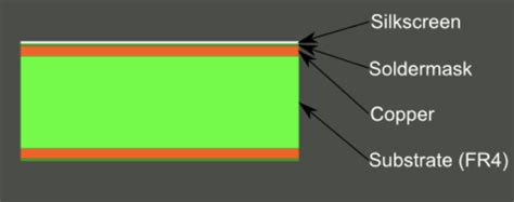
What is PCB Silkscreen?
PCB silkscreen, also known as legend or nomenclature, is the text and symbols printed on the surface of a printed circuit board (PCB) to provide information about the board’s components, assembly instructions, and other important details. The silkscreen layer is typically applied using a screen printing process, which involves pushing ink through a fine mesh screen onto the PCB surface.
Importance of PCB Silkscreen
PCB silkscreen serves several critical functions:
-
Component identification: Silkscreen labels help identify components, their values, and their orientation, making it easier for technicians to assemble and troubleshoot the board.
-
Assembly instructions: Silkscreen can provide information on the proper placement and orientation of components, as well as any special handling instructions.
-
Branding and aesthetics: Silkscreen can be used to add logos, product names, and other branding elements to the PCB, enhancing its visual appeal.
-
Regulatory compliance: Silkscreen can include mandatory markings, such as UL or CE symbols, to indicate compliance with safety and regulatory standards.
Key Considerations for PCB Silkscreen Design
When designing PCB silkscreen, several factors must be taken into account to ensure readability, clarity, and manufacturability.
Font Selection
Choosing the right font for PCB silkscreen is crucial for legibility. Some guidelines for font selection include:
- Use a sans-serif font, such as Arial or Helvetica, for better readability.
- Ensure the font is compatible with the silkscreen printing process.
- Select a font size that is large enough to be easily read, typically 0.8mm or larger.
| Font | Minimum Size | Recommended Size |
|---|---|---|
| Arial | 0.6mm | 0.8mm |
| Helvetica | 0.6mm | 0.8mm |
| Verdana | 0.7mm | 0.9mm |
| Tahoma | 0.7mm | 0.9mm |
Character Spacing and Line Width
Proper character spacing and line width are essential for silkscreen legibility. The following guidelines should be followed:
- Maintain a minimum space of 0.15mm between characters.
- Keep a minimum line width of 0.15mm for best results.
- Avoid placing silkscreen too close to pads or other features, maintaining a clearance of at least 0.3mm.
Orientation and Placement
When placing silkscreen on the PCB, consider the following:
- Orient text to be easily read from left to right or bottom to top.
- Place silkscreen on the component side of the board, unless otherwise specified.
- Avoid placing silkscreen over pads, vias, or other conductive features.
- Ensure silkscreen does not interfere with component placement or soldering.
Color and Contrast
Silkscreen color and contrast play a role in readability and aesthetics:
- White silkscreen on a dark background (e.g., green or black) provides the best contrast and readability.
- Yellow silkscreen can be used for warning or caution messages.
- Other colors, such as red or blue, may be used for decorative purposes but should be used sparingly to avoid confusion.

Common PCB Silkscreen Symbols and Their Meanings
PCB silkscreen often includes standard symbols to convey information about components and their orientation. Some common symbols include:
| Symbol | Meaning |
|---|---|
| + | Positive voltage or pin |
| – | Negative voltage or pin |
| • | Through-hole pad |
| ◦ | Surface-mount pad |
| ▷ | Input pin |
| ◁ | Output pin |
| 1, 2, 3 | Pin numbers |

PCB Silkscreen Design Workflow
The PCB silkscreen design process typically involves the following steps:
- Create the silkscreen layer in the PCB design software, such as Altium Designer or KiCad.
- Add text, symbols, and logos to the silkscreen layer, following the guidelines for font selection, spacing, and placement.
- Review the silkscreen design for clarity, legibility, and manufacturability.
- Generate the silkscreen Gerber file for manufacturing.
- Verify the silkscreen design with the PCB manufacturer to ensure compatibility with their processes.

FAQ
-
Q: Can silkscreen be applied to both sides of the PCB?
A: Yes, silkscreen can be applied to both the component side and the solder side of the PCB. However, it is more common to place silkscreen on the component side for better visibility during assembly. -
Q: What is the minimum size for silkscreen text?
A: The minimum recommended size for silkscreen text is 0.8mm. Smaller text may be possible but can lead to reduced legibility. -
Q: Can silkscreen be used for soldermask?
A: No, silkscreen and soldermask are two separate layers in PCB design. Soldermask is used to protect the copper traces from oxidation and prevent solder bridges, while silkscreen is used for labeling and information. -
Q: Are there any limitations on the colors available for silkscreen?
A: Most PCB manufacturers offer a limited range of standard silkscreen colors, such as white, yellow, and black. Custom colors may be available but can increase costs and lead times. -
Q: Can silkscreen be removed or modified after the PCB is manufactured?
A: Removing or modifying silkscreen after manufacturing is difficult and not recommended. Any changes to the silkscreen should be made during the design phase before the PCB is sent for production.
In conclusion, PCB silkscreen is a critical element of PCB design, providing essential information for assembly, troubleshooting, and identification. By following best practices for font selection, spacing, placement, and color, designers can create clear, legible, and visually appealing silkscreens that enhance the overall quality and functionality of their PCBs.
[Word count: 970]


Leave a Reply