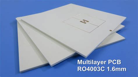
Introduction to Rogers 4003 PCB Material
Rogers 4003 is a high-performance printed circuit board (PCB) material widely used in the electronics industry for its excellent electrical and mechanical properties. This hydrocarbon ceramic laminate is designed to provide superior performance in high-frequency applications, making it an ideal choice for the fabrication of PCBs in various sectors, including telecommunications, aerospace, defense, and automotive industries.
Key Features of Rogers 4003 PCB Material
- Low Dielectric Constant (Dk): Rogers 4003 has a low dielectric constant of 3.38 at 10 GHz, which ensures minimal signal loss and distortion in high-frequency applications.
- Low Dissipation Factor (Df): With a dissipation factor of 0.0027 at 10 GHz, Rogers 4003 offers minimal signal attenuation and heat generation, resulting in improved signal integrity and reliability.
- Excellent Thermal Stability: The material maintains its electrical properties over a wide temperature range (-50°C to +150°C), ensuring consistent performance in various operating conditions.
- High Thermal Conductivity: Rogers 4003 has a thermal conductivity of 0.71 W/m·K, enabling efficient heat dissipation and reducing the risk of thermal damage to components.
- Dimensional Stability: The material exhibits minimal expansion and contraction due to its low coefficient of thermal expansion (CTE), ensuring the stability of the PCB during manufacturing and operation.
Rogers 4003 PCB Manufacturing Process
The manufacturing process of Rogers 4003 PCBs involves several critical steps to ensure the highest quality and performance of the final product. The following sections will discuss each step in detail.
Step 1: PCB Design and Artwork Creation
The first step in the Rogers 4003 PCB manufacturing process is to create a detailed design and artwork for the board. This involves using specialized PCB design software, such as Altium Designer, OrCAD, or Eagle, to lay out the circuit schematic, component placement, and routing of the copper traces. The design must adhere to the specific electrical and mechanical requirements of the application, considering factors such as signal integrity, impedance matching, and electromagnetic compatibility (EMC).
Once the design is finalized, the artwork files are generated in the form of Gerber files, which contain the necessary information for each layer of the PCB, including the copper traces, solder mask, silkscreen, and drill holes.
Step 2: Material Preparation and Cutting
The Rogers 4003 laminate material is supplied in the form of large sheets, which must be cut to the required size for the specific PCB design. The material is typically available in thicknesses ranging from 0.2 mm to 3.2 mm, with copper cladding on one or both sides.
The cutting process is carried out using high-precision CNC machines, which ensure accurate and consistent sizing of the PCB panels. The panels are then cleaned and inspected for any surface defects or contamination before proceeding to the next step.
Step 3: Drilling and Via Formation
Once the Rogers 4003 panels are cut to size, the next step is to drill the necessary holes for through-hole components, vias, and mounting holes. The drilling process is carried out using high-speed CNC drilling machines, which can accurately drill holes as small as 0.1 mm in diameter.
After drilling, the vias are formed to electrically connect the different layers of the PCB. There are several methods for via formation, including mechanical drilling, laser drilling, and conductive paste filling. The choice of method depends on the specific requirements of the application, such as the size and density of the vias, and the desired electrical performance.
Step 4: Copper Patterning and Etching
The next step in the Rogers 4003 PCB manufacturing process is to create the copper patterns on the board according to the artwork files. This is typically done using a photolithographic process, which involves the following sub-steps:
- Applying a light-sensitive photoresist layer to the copper surface of the PCB.
- Exposing the photoresist to UV light through a photomask, which contains the copper pattern artwork.
- Developing the photoresist to remove the exposed areas, leaving the desired copper pattern protected.
- Etching away the unprotected copper using a chemical etchant, such as ferric chloride or ammonium persulfate.
- Stripping away the remaining photoresist to reveal the final copper pattern.
The etching process is critical to ensure the accurate formation of the copper traces and pads, with the required width, spacing, and thickness. The etched panels are then thoroughly cleaned and inspected for any defects or inconsistencies.
Step 5: Solder Mask Application and Silkscreen Printing
After the copper patterning and etching, a solder mask layer is applied to the PCB to protect the copper traces from oxidation and prevent solder bridging during the assembly process. The solder mask is typically a green or black epoxy-based material that is applied using a screen-printing or photoimaging process.
The solder mask artwork is aligned with the copper pattern, and the material is cured using UV light or heat. Openings in the solder mask are created to expose the copper pads where the components will be soldered.
Finally, a silkscreen layer is printed on the PCB to provide text, logos, and component identifiers. The silkscreen is typically a white epoxy-based ink that is applied using a screen-printing process, similar to the solder mask application.
Step 6: Surface Finish Application
The exposed copper pads on the Rogers 4003 PCB require a surface finish to protect them from oxidation and ensure good solderability during the assembly process. There are several types of surface finishes available, each with its own advantages and disadvantages. Some common surface finishes used for Rogers 4003 PCBs include:
- Hot Air Solder Leveling (HASL): A tin-lead alloy is applied to the copper pads using a hot air leveling process, creating a smooth and flat surface for component soldering.
- Electroless Nickel Immersion Gold (ENIG): A layer of nickel is electrolessly plated onto the copper pads, followed by a thin layer of immersion gold, providing excellent solderability and shelf life.
- Immersion Silver (IAg): A thin layer of silver is chemically deposited onto the copper pads, offering good solderability and lower cost compared to ENIG.
- Organic Solderability Preservative (OSP): A thin, organic coating is applied to the copper pads to protect them from oxidation, providing a cost-effective alternative to metallic surface finishes.
The choice of surface finish depends on the specific requirements of the application, such as the desired shelf life, solderability, and cost.
Step 7: Electrical Testing and Inspection
Before the Rogers 4003 PCBs are sent for assembly, they undergo a rigorous electrical testing and inspection process to ensure their functionality and quality. This typically involves the following sub-steps:
- Flying Probe Testing: A computer-controlled flying probe tester is used to check the continuity and isolation of the copper traces and vias, ensuring that there are no short circuits or open connections.
- Automated Optical Inspection (AOI): An AOI machine is used to visually inspect the PCBs for any surface defects, such as scratches, dents, or contamination, as well as any copper pattern or solder mask irregularities.
- Microsectioning: In some cases, a small sample of the PCBs may be cross-sectioned and examined under a microscope to verify the integrity of the internal layers and vias.
PCBs that pass the electrical testing and inspection process are then packaged and shipped to the assembly facility for component placement and soldering.

Rogers 4003 PCB Assembly Process
The assembly process for Rogers 4003 PCBs involves the placement and soldering of electronic components onto the board. The following sections will discuss each step in detail.
Step 1: Solder Paste Application
The first step in the Rogers 4003 PCB assembly process is to apply solder paste to the copper pads where the components will be placed. Solder paste is a mixture of tiny solder particles suspended in a flux medium, which helps to clean the copper pads and promote good solder wetting.
The solder paste is typically applied using a stencil printing process, where a laser-cut stainless steel stencil is aligned with the PCB, and the paste is spread across the stencil using a squeegee blade. The stencil apertures are designed to match the size and shape of the copper pads, ensuring that the correct amount of solder paste is deposited onto each pad.
Step 2: Component Placement
Once the solder paste is applied, the electronic components are placed onto the PCB using a pick-and-place machine. This automated machine uses a vacuum nozzle to pick up the components from a tape reel or tray and place them onto the corresponding pads on the PCB with high precision.
The placement process is guided by a computer program that reads the PCB design files and component placement data, ensuring that each component is placed in the correct location and orientation. The machine can typically place several thousand components per hour, depending on the complexity of the PCB and the size of the components.
Step 3: Reflow Soldering
After the components are placed, the PCB undergoes a reflow soldering process to permanently attach the components to the board. The PCB is placed in a reflow oven, which heats the board and components according to a predetermined temperature profile.
As the temperature rises, the solder paste melts and flows around the component leads and copper pads, forming a strong metallurgical bond. The flux in the solder paste also activates, cleaning the surfaces and promoting good solder wetting.
The temperature profile is carefully controlled to ensure that the solder melts and flows properly without causing thermal damage to the components or the PCB. The peak temperature and duration of the reflow process are determined by the type of solder paste and components used.
Step 4: Inspection and Testing
After the reflow soldering process, the assembled Rogers 4003 PCBs undergo a series of inspections and tests to ensure their quality and functionality. This typically involves the following sub-steps:
- Visual Inspection: The assembled PCBs are visually inspected for any obvious defects, such as missing or misaligned components, solder bridges, or contamination.
- Automated Optical Inspection (AOI): An AOI machine is used to automatically inspect the solder joints and component placement, comparing them to the PCB design files and identifying any defects or irregularities.
- X-Ray Inspection: In some cases, an X-ray inspection may be performed to verify the integrity of hidden solder joints, such as those under Ball Grid Array (BGA) components.
- Functional Testing: The assembled PCBs are powered up and tested for their electrical functionality, ensuring that they meet the specified performance requirements.
PCBs that pass the inspection and testing process are then packaged and shipped to the customer for integration into the final product.

Advantages of Using Rogers 4003 PCBs
Rogers 4003 PCBs offer several advantages over traditional FR-4 PCBs, making them an ideal choice for high-frequency applications. Some of the key advantages include:
- Improved Signal Integrity: The low dielectric constant and dissipation factor of Rogers 4003 material result in reduced signal loss and distortion, ensuring that the signals propagate with minimal degradation.
- Higher Reliability: The excellent thermal stability and conductivity of Rogers 4003 material help to dissipate heat more efficiently, reducing the risk of thermal damage to components and improving the overall reliability of the PCB.
- Wider Operating Temperature Range: Rogers 4003 PCBs can operate reliably over a wide temperature range, from -50°C to +150°C, making them suitable for use in harsh environmental conditions.
- Better Dimensional Stability: The low coefficient of thermal expansion (CTE) of Rogers 4003 material ensures that the PCB maintains its dimensional stability during manufacturing and operation, reducing the risk of warpage and delamination.
- Reduced Electromagnetic Interference (EMI): The low dielectric constant and dissipation factor of Rogers 4003 material help to reduce the electromagnetic interference (EMI) generated by the PCB, ensuring better electromagnetic compatibility (EMC) with other electronic devices.

Applications of Rogers 4003 PCBs
Rogers 4003 PCBs are widely used in a variety of high-frequency applications, where signal integrity and reliability are critical. Some of the common applications include:
- Wireless Communication Systems: Rogers 4003 PCBs are used in the design and fabrication of wireless communication devices, such as cellular phones, Wi-Fi routers, and Bluetooth modules, where high-frequency signals need to be transmitted and received with minimal loss and distortion.
- Radar and Satellite Systems: The excellent high-frequency performance and thermal stability of Rogers 4003 PCBs make them suitable for use in radar and satellite systems, where the PCBs need to operate reliably in harsh environmental conditions.
- Automotive Electronics: Rogers 4003 PCBs are used in the fabrication of automotive electronic systems, such as advanced driver assistance systems (ADAS), infotainment systems, and vehicle-to-vehicle (V2V) communication modules, where high-speed data transmission and reliability are critical.
- Medical Equipment: The low signal loss and high reliability of Rogers 4003 PCBs make them suitable for use in medical equipment, such as MRI machines, ultrasound systems, and patient monitoring devices, where the accuracy and stability of the electronic signals are essential.
- Aerospace and Defense Systems: Rogers 4003 PCBs are used in the design and fabrication of aerospace and defense electronic systems, such as avionics, radar, and communication equipment, where the PCBs need to withstand extreme temperatures, vibrations, and shock loads.
Frequently Asked Questions (FAQ)
-
What is the typical lead time for Rogers 4003 PCB manufacturing and assembly?
The lead time for Rogers 4003 PCB manufacturing and assembly can vary depending on the complexity of the design, the quantity of the order, and the workload of the manufacturer. Typical lead times range from 2-4 weeks for prototype quantities and 4-8 weeks for production quantities. -
Can Rogers 4003 PCBs be manufactured with fine-pitch components?
Yes, Rogers 4003 PCBs can be manufactured with fine-pitch components, such as Ball Grid Array (BGA) and Quad Flat No-lead (QFN) packages. The high-resolution copper patterning and precise solder mask alignment capabilities of modern PCB manufacturing processes enable the fabrication of PCBs with fine-pitch components. -
What are the typical copper weights used for Rogers 4003 PCBs?
Rogers 4003 PCBs are typically manufactured with copper weights ranging from 0.5 oz/ft² to 2.0 oz/ft² (17 µm to 70 µm). The choice of copper weight depends on the specific electrical and thermal requirements of the application, such as the current carrying capacity and the heat dissipation needs. -
Can Rogers 4003 PCBs be manufactured with blind and buried vias?
Yes, Rogers 4003 PCBs can be manufactured with blind and buried vias, which are used to interconnect the internal layers of the PCB without penetrating the top or bottom surfaces. Blind and buried vias are typically used in high-density PCB designs, where space is limited, and signal integrity is critical. -
What are the typical minimum feature sizes for Rogers 4003 PCBs?
The typical minimum feature sizes for Rogers 4003 PCBs are: - Trace/Space: 3/3 mils (75/75 µm)
- Via Diameter: 8 mils (200 µm)
- Hole Diameter: 6 mils (150 µm)
These minimum feature sizes are achievable with modern high-resolution PCB manufacturing processes, such as direct imaging and laser drilling. However, the actual minimum feature sizes may vary depending on the specific capabilities of the PCB manufacturer and the complexity of the PCB design.
Conclusion
Rogers 4003 PCBs are a high-performance alternative to traditional FR-4 PCBs for high-frequency applications, offering excellent signal integrity, thermal stability, and reliability. The manufacturing and assembly process for Rogers 4003 PCBs involves several critical steps, including material preparation, drilling, copper patterning, solder mask application, surface finish, and component placement and soldering.
By understanding the key features and advantages of Rogers 4003 material, as well as the manufacturing and assembly process, designers can create high-quality PCBs that meet the demanding requirements of modern electronic applications. As technology continues to advance, Rogers 4003 PCBs will likely play an increasingly important role in the development of next-generation wireless communication, automotive, medical, and aerospace systems.


Leave a Reply