Introduction to PCB Warpage Measurement
In the world of printed circuit board (PCB) manufacturing, warpage has become a critical issue that can significantly impact the reliability and functionality of electronic devices. PCB warpage refers to the distortion or bending of a PCB during the reflow soldering process, which can lead to various problems such as component misalignment, poor solder joint formation, and even device failure. To address this issue, the IPC (Association Connecting Electronics Industries) has introduced the new IPC-9641 standard, which provides guidelines for measuring and characterizing PCB warpage during reflow.
In this article, we will explore the importance of PCB warpage measurement, the key aspects of the IPC-9641 standard, and how to effectively implement it in your manufacturing process.
Why Measure PCB Warpage?
The Impact of PCB Warpage on Electronic Devices
PCB warpage can have a significant impact on the quality and reliability of electronic devices. When a PCB undergoes excessive warpage during reflow, it can lead to several issues, including:
- Component misalignment: Warped PCBs can cause components to shift from their intended positions, resulting in misalignment and potential short circuits.
- Poor solder joint formation: Excessive warpage can prevent proper contact between the PCB and components, leading to weak or incomplete solder joints.
- Stress on components: Warpage can induce mechanical stress on components, potentially causing damage or premature failure.
- Reduced reliability: Devices with warped PCBs are more likely to experience failures or malfunctions, reducing overall reliability.
By measuring and controlling PCB warpage, manufacturers can minimize these issues and ensure the production of high-quality, reliable electronic devices.
The Benefits of Implementing IPC-9641
Adopting the IPC-9641 standard for PCB warpage measurement offers several benefits to manufacturers, including:
- Improved product quality: By accurately measuring and characterizing PCB warpage, manufacturers can identify and address issues early in the production process, leading to improved overall product quality.
- Increased reliability: Controlling PCB warpage helps ensure proper component attachment and solder joint formation, resulting in more reliable electronic devices.
- Cost savings: Identifying and resolving warpage issues early can reduce the need for rework, scrap, and warranty claims, ultimately saving costs for manufacturers.
- Standardized measurement: IPC-9641 provides a standardized method for measuring PCB warpage, allowing for consistent and comparable results across different manufacturing facilities and equipment.

Understanding the IPC-9641 Standard
Key Aspects of IPC-9641
The IPC-9641 standard, titled “Measurement and Characterization of PCB Warpage during Reflow,” provides a comprehensive set of guidelines for measuring and reporting PCB warpage during the reflow soldering process. Some of the key aspects of the standard include:
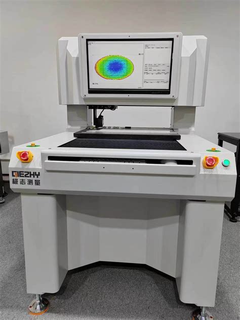
- Measurement techniques: IPC-9641 specifies the use of shadow moiré or laser scanning techniques for measuring PCB warpage.
- Sample preparation: The standard outlines requirements for sample preparation, including the number of samples, conditioning, and handling procedures.
- Measurement parameters: IPC-9641 defines the measurement parameters, such as the number of measurement points, spacing, and location on the PCB.
- Reporting requirements: The standard provides guidelines for reporting measurement results, including data format, units, and statistical analysis.
By following these guidelines, manufacturers can ensure accurate and consistent measurement of PCB warpage, allowing for better process control and product quality.
Measurement Techniques: Shadow Moiré and Laser Scanning
IPC-9641 specifies two primary techniques for measuring PCB warpage during reflow: shadow moiré and laser scanning.
- Shadow moiré: This technique involves projecting a grid pattern onto the PCB surface and observing the resulting moiré fringes. The fringes represent contours of equal warpage, allowing for quantitative measurement of the PCB’s distortion.
- Laser scanning: This method uses a laser sensor to scan the PCB surface, creating a 3D point cloud that represents the PCB’s shape. The point cloud data is then analyzed to determine the extent and distribution of warpage.
Both techniques have their advantages and limitations, and the choice of method may depend on factors such as equipment availability, PCB size, and required resolution.

Implementing IPC-9641 in Your Manufacturing Process
Steps for Adopting IPC-9641
To successfully implement the IPC-9641 standard in your manufacturing process, follow these steps:
- Acquire the necessary equipment: Invest in shadow moiré or laser scanning equipment that meets the requirements specified in IPC-9641.
- Train personnel: Ensure that your staff is trained in the proper use of the measurement equipment and the IPC-9641 guidelines.
- Establish a measurement plan: Develop a plan that outlines the frequency of measurements, sample size, and reporting procedures based on the IPC-9641 standard.
- Integrate with existing processes: Incorporate PCB warpage measurement into your existing quality control and process improvement initiatives.
- Analyze and act on results: Regularly review the measurement data, identify trends or issues, and take appropriate actions to optimize your reflow soldering process and minimize PCB warpage.
Best Practices for PCB Warpage Control
In addition to measuring PCB warpage, manufacturers can employ several best practices to minimize warpage and improve product quality:
- Material selection: Choose PCB materials with low coefficient of thermal expansion (CTE) and good dimensional stability to reduce warpage potential.
- Design optimization: Incorporate design features that minimize warpage, such as balanced copper distribution, symmetrical layer stackup, and proper component placement.
- Process control: Optimize reflow soldering parameters, such as peak temperature, ramp rates, and cooling rates, to minimize thermal stress on the PCB.
- Moisture management: Implement proper storage and handling procedures to control moisture absorption in PCBs, as moisture can contribute to warpage during reflow.
By combining these best practices with regular PCB warpage measurement using the IPC-9641 standard, manufacturers can effectively control warpage and ensure the production of high-quality, reliable electronic devices.

Conclusion
PCB warpage is a critical issue in electronic manufacturing that can significantly impact product quality and reliability. By adopting the IPC-9641 standard for measuring and characterizing PCB warpage during reflow, manufacturers can gain valuable insights into their processes and take proactive steps to minimize warpage-related issues. Implementing the standard, along with best practices for PCB warpage control, can lead to improved product quality, increased reliability, and cost savings for manufacturers.
As the electronics industry continues to evolve, with increasingly complex designs and higher performance requirements, the importance of PCB warpage measurement and control will only grow. By staying up-to-date with standards like IPC-9641 and investing in the necessary equipment and training, manufacturers can position themselves to meet the challenges of the future and deliver high-quality, reliable electronic devices to their customers.
FAQ
-
What is PCB warpage, and why is it important to measure?
PCB warpage is the distortion or bending of a PCB during the reflow soldering process. It is important to measure because excessive warpage can lead to component misalignment, poor solder joint formation, and reduced device reliability. -
What are the two primary techniques for measuring PCB warpage specified in IPC-9641?
The two primary techniques for measuring PCB warpage specified in IPC-9641 are shadow moiré and laser scanning. Shadow moiré involves projecting a grid pattern onto the PCB surface and observing the resulting moiré fringes, while laser scanning uses a laser sensor to create a 3D point cloud representing the PCB’s shape. -
How can manufacturers implement the IPC-9641 standard in their manufacturing process?
To implement the IPC-9641 standard, manufacturers should acquire the necessary measurement equipment, train their personnel, establish a measurement plan, integrate the measurement process with existing quality control initiatives, and regularly analyze and act on the results. -
What are some best practices for PCB warpage control?
Best practices for PCB warpage control include selecting materials with low CTE and good dimensional stability, optimizing PCB design to minimize warpage, controlling reflow soldering parameters, and implementing proper moisture management procedures. -
How can adopting the IPC-9641 standard benefit manufacturers?
Adopting the IPC-9641 standard can benefit manufacturers by improving product quality, increasing reliability, reducing costs associated with rework and scrap, and providing a standardized method for measuring PCB warpage that allows for consistent and comparable results across different manufacturing facilities and equipment.
| Parameter | Shadow Moiré | Laser Scanning |
|---|---|---|
| Measurement Principle | Projection of grid pattern and observation of moiré fringes | Laser sensor scanning and creation of 3D point cloud |
| Resolution | Depends on grid pitch and camera resolution | Depends on laser spot size and scanning resolution |
| Speed | Relatively fast, suitable for inline measurement | Slower than shadow moiré, better suited for offline measurement |
| Cost | Generally lower cost compared to laser scanning | Higher cost due to more complex equipment |
| Limitations | Limited depth resolution, may struggle with highly reflective surfaces | May have issues with transparent or translucent materials |
Table 1: Comparison of shadow moiré and laser scanning techniques for PCB warpage measurement.


Leave a Reply