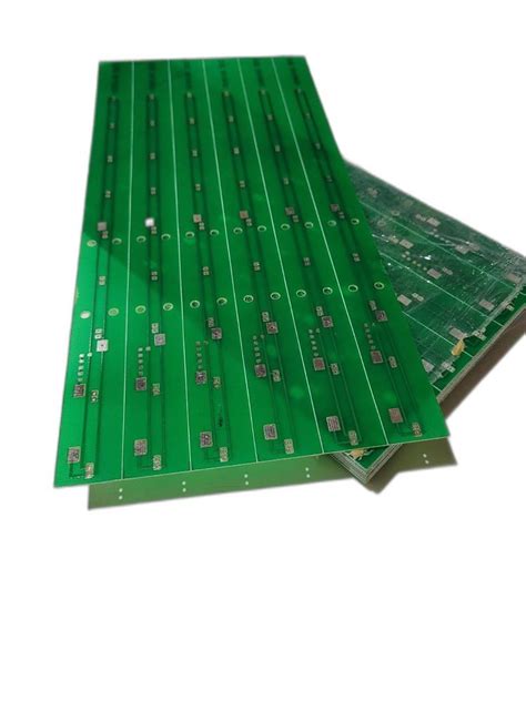
What is PCB Fabrication?
PCB fabrication is the process of manufacturing printed circuit boards (PCBs) that are used in various electronic devices. The process involves several steps, including designing the circuit, creating the PCB layout, printing the circuit onto the board, and assembling the components onto the board.
The PCB Fabrication Process
The PCB fabrication process typically involves the following steps:
-
Design: The first step in PCB fabrication is to design the circuit using specialized software. This involves creating a schematic diagram of the circuit and then converting it into a PCB layout.
-
Material Selection: Once the design is complete, the next step is to select the appropriate material for the PCB. The most common materials used in PCB fabrication are FR-4, which is a glass-reinforced epoxy laminate, and polyimide, which is a high-temperature resistant material.
-
Printing: After the material is selected, the next step is to print the circuit onto the board. This is typically done using a process called photolithography, which involves exposing the board to light through a photomask and then developing the exposed areas.
-
Etching: Once the circuit is printed onto the board, the next step is to etch away the unwanted copper to leave only the desired circuit pattern. This is typically done using a chemical etching process.
-
Drilling: After the etching process is complete, the next step is to drill holes in the board for the components to be mounted. This is typically done using a computer-controlled drill.
-
Plating: Once the holes are drilled, the next step is to plate the holes and the circuit pattern with a thin layer of copper to improve the conductivity and durability of the board.
-
Solder Mask: After the plating process is complete, a solder mask is applied to the board to protect the copper from oxidation and to prevent solder bridges from forming during the assembly process.
-
Silkscreen: The final step in the PCB fabrication process is to apply a silkscreen to the board, which is used to label the components and provide other information about the board.
Types of PCBs
There are several types of PCBs, each with its own unique characteristics and applications. The most common types of PCBs are:
Single-Sided PCBs
Single-sided PCBs have components and circuits on only one side of the board. They are the simplest and least expensive type of PCB, but they have limited functionality and are typically used in low-cost consumer electronics.
Double-Sided PCBs
Double-sided PCBs have components and circuits on both sides of the board, which allows for more complex circuits and higher component density. They are more expensive than single-sided PCBs but offer better performance and reliability.
Multi-Layer PCBs
Multi-layer PCBs have multiple layers of circuits stacked on top of each other, separated by insulating layers. They are the most complex and expensive type of PCB but offer the highest level of performance and functionality. Multi-layer PCBs are typically used in high-end electronics, such as smartphones, computers, and medical devices.
Flexible PCBs
Flexible PCBs are made from flexible materials, such as polyimide, and can be bent or folded to fit into tight spaces. They are often used in wearable electronics, such as smartwatches and fitness trackers, and in applications where the PCB needs to be flexible, such as in automotive and aerospace electronics.
Rigid-Flex PCBs
Rigid-flex PCBs are a combination of rigid and flexible PCBs, where the rigid sections are used for mounting components and the flexible sections are used for connecting the rigid sections. They offer the benefits of both rigid and flexible PCBs and are often used in applications where space is limited, such as in medical devices and aerospace electronics.

PCB Materials
The choice of material for a PCB is critical to its performance and reliability. The most common materials used in PCB fabrication are:
FR-4
FR-4 is a glass-reinforced epoxy laminate that is the most widely used material for PCBs. It is inexpensive, has good mechanical and electrical properties, and is easy to work with. FR-4 is suitable for most applications, but it may not be suitable for high-frequency or high-temperature applications.
Polyimide
Polyimide is a high-temperature resistant material that is often used in applications where the PCB needs to withstand high temperatures, such as in automotive and aerospace electronics. It is more expensive than FR-4 but offers better thermal and chemical resistance.
Teflon
Teflon is a low-loss material that is often used in high-frequency applications, such as in RF and microwave electronics. It has excellent dielectric properties and is resistant to moisture and chemicals, but it is more expensive than other materials.
Ceramic
Ceramic is a high-performance material that is often used in high-power and high-frequency applications, such as in power electronics and RF electronics. It has excellent thermal and electrical properties but is more expensive and difficult to work with than other materials.

PCB Assembly
After the PCB fabrication process is complete, the next step is to assemble the components onto the board. PCB assembly typically involves the following steps:
-
Solder Paste Application: The first step in PCB assembly is to apply solder paste to the pads on the board where the components will be mounted. This is typically done using a stencil and a squeegee.
-
Component Placement: Once the solder paste is applied, the next step is to place the components onto the board. This is typically done using a pick-and-place machine, which uses a vacuum nozzle to pick up the components and place them onto the board.
-
Reflow Soldering: After the components are placed onto the board, the next step is to heat the board to melt the solder paste and create a permanent connection between the components and the board. This is typically done using a reflow oven, which heats the board to a specific temperature profile.
-
Inspection: Once the reflow soldering process is complete, the next step is to inspect the board for any defects or issues. This is typically done using automated optical inspection (AOI) equipment, which uses cameras and image processing software to detect any problems.
-
Testing: The final step in PCB assembly is to test the board to ensure that it functions correctly. This is typically done using functional testing equipment, which tests the board under various operating conditions to ensure that it meets the required specifications.

PCB Design Considerations
When designing a PCB, there are several important considerations to keep in mind to ensure that the board functions correctly and reliably. Some of the key design considerations include:
Signal Integrity
Signal integrity refers to the quality of the electrical signals traveling through the PCB. To ensure good signal integrity, the PCB should be designed with proper grounding, shielding, and impedance matching techniques. This is particularly important for high-frequency and high-speed applications.
Thermal Management
Thermal management refers to the ability of the PCB to dissipate heat generated by the components. To ensure good thermal management, the PCB should be designed with adequate cooling mechanisms, such as heatsinks, fans, or thermal vias. This is particularly important for high-power applications.
Electromagnetic Compatibility (EMC)
EMC refers to the ability of the PCB to operate without causing or being affected by electromagnetic interference (EMI). To ensure good EMC, the PCB should be designed with proper shielding, filtering, and grounding techniques. This is particularly important for applications that are sensitive to EMI, such as medical devices and aerospace electronics.
Manufacturing Considerations
When designing a PCB, it is important to consider the manufacturing process and the limitations of the fabrication equipment. This includes considerations such as minimum trace width and spacing, hole size and spacing, and component placement. Failure to consider these limitations can result in manufacturing defects and reduced reliability.
Frequently Asked Questions (FAQ)
What is the difference between a PCB and a PCBA?
A PCB (printed circuit board) is the bare board without any components mounted on it, while a PCBA (printed circuit board assembly) is the board with all the components mounted and soldered onto it.
What is the typical turnaround time for PCB fabrication?
The turnaround time for PCB fabrication varies depending on the complexity of the board and the fabrication process used. For simple single-sided or double-sided boards, the turnaround time can be as short as 24 hours, while for complex multi-layer boards, it can take several weeks.
What is the minimum trace width and spacing for PCB fabrication?
The minimum trace width and spacing for PCB fabrication depends on the fabrication process and the equipment used. For standard PCB fabrication processes, the minimum trace width and spacing is typically around 0.1mm (4 mils), while for high-density interconnect (HDI) processes, it can be as small as 0.05mm (2 mils).
Can PCBs be recycled?
Yes, PCBs can be recycled, but the process is complex and requires specialized equipment and processes. PCBs contain valuable metals such as gold, silver, and copper, as well as hazardous materials such as lead and brominated flame retardants, which must be properly separated and disposed of. Recycling PCBs can help reduce electronic waste and conserve natural resources.
What is the difference between reflow soldering and wave soldering?
Reflow soldering and wave soldering are two common methods used for PCB assembly. Reflow soldering involves applying solder paste to the board and then heating the board in a reflow oven to melt the solder and create a permanent connection between the components and the board. Wave soldering involves passing the board over a wave of molten solder, which creates a connection between the components and the board. Reflow soldering is typically used for surface mount components, while wave soldering is used for through-hole components.


Leave a Reply