Introduction to QFN Packaging
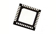
QFN (Quad Flat No-lead) packaging is a surface-mount technology that has gained popularity in recent years due to its numerous advantages over traditional packaging methods. QFN packages are characterized by their small size, excellent thermal and electrical performance, and cost-effectiveness. In this comprehensive article, we will explore the various types of QFN packaging, the assembly process, and the benefits they offer in modern electronics design.
Types of QFN Packaging
Standard QFN Packages
Standard QFN packages are the most common type of QFN packaging. They feature a square or rectangular body with exposed pads on the bottom surface for thermal and electrical contact. The lead count for standard QFN packages typically ranges from 16 to 200, with body sizes varying from 2mm x 2mm to 12mm x 12mm.
Dual Row QFN Packages
Dual row QFN packages, also known as DRQFN or QFN-DR, offer a higher lead count within a given package size compared to standard QFN packages. This is achieved by arranging the leads in two rows along the perimeter of the package. Dual row QFN packages are suitable for applications that require a higher pin count without increasing the package footprint.
Thermally Enhanced QFN Packages
Thermally enhanced QFN packages, or TQFN, are designed to improve heat dissipation in high-power applications. These packages feature a larger exposed pad on the bottom surface, which acts as a heat sink to efficiently transfer heat away from the die. TQFN packages are commonly used in power management ICs, RF devices, and other applications that generate significant heat.
Punch QFN Packages
Punch QFN packages, also known as PQFN, are manufactured using a punching process instead of the traditional etching method. This results in a more robust and reliable package with better mechanical strength. Punch QFN packages are often used in automotive and industrial applications that require high reliability and durability.

QFN Package Assembly Process
The assembly process for QFN packages involves several key steps to ensure proper attachment and functionality of the device. Here’s a detailed overview of the QFN package assembly process:
-
Solder Paste Printing: Solder paste is applied to the PCB Pads using a stencil printing process. The stencil ensures that the correct amount of solder paste is deposited on each pad.
-
Component Placement: The QFN package is placed onto the PCB using a pick-and-place machine. The machine aligns the package with the solder paste-covered pads on the PCB.
-
Reflow Soldering: The PCB with the placed QFN package undergoes a reflow soldering process. The assembly is heated to a specific temperature profile, causing the solder paste to melt and form a strong bond between the package leads and the PCB PADS.
-
Inspection: After the reflow soldering process, the assembLED PCB undergoes visual and automated optical inspection (AOI) to ensure proper solder joint formation and detect any defects or misalignments.
-
Underfill Application (Optional): In some cases, an underfill material is applied between the QFN package and the PCB to improve mechanical strength and thermal performance. The underfill helps to distribute stress and prevent solder joint fatigue caused by thermal expansion mismatches.
-
Testing: The assembled PCB undergoes various electrical and functional tests to verify the performance and reliability of the QFN package and the overall circuit.

Benefits of QFN Packaging
QFN packaging offers several significant benefits over traditional packaging methods, making it an attractive choice for modern electronics design:
-
Reduced Package Size: QFN packages have a smaller footprint compared to traditional lead frame-based packages, allowing for higher component density and more compact device designs.
-
Improved Thermal Performance: The exposed pad on the bottom of QFN packages provides an efficient thermal path for heat dissipation, enabling better thermal management and increased power handling capability.
-
Enhanced Electrical Performance: The shorter lead lengths and reduced package parasitics in QFN packages result in improved electrical performance, including lower inductance, lower resistance, and better high-frequency characteristics.
-
Cost-Effectiveness: QFN packaging is generally more cost-effective compared to other packaging technologies due to its simpler design, reduced material usage, and compatibility with standard SMT Assembly processes.
-
Increased Reliability: The robust construction and good mechanical strength of QFN packages contribute to enhanced reliability and durability, making them suitable for demanding applications in various industries.

QFN Package Design Considerations
When designing circuits using QFN packages, there are several key considerations to ensure optimal performance and manufacturability:
-
PCB Layout: Proper PCB layout is crucial for QFN packages to ensure good signal integrity, thermal management, and manufacturability. Designers should follow recommended layout guidelines, including pad sizes, spacing, and thermal vias.
-
Thermal Management: Adequate thermal management is essential for QFN packages, especially in high-power applications. Designers should consider factors such as the exposed pad size, thermal vias, and heatsink design to effectively dissipate heat from the package.
-
Signal Integrity: QFN packages offer good high-frequency performance, but proper signal integrity practices must be followed to minimize crosstalk, reflection, and other signal quality issues. This includes proper impedance matching, ground plane design, and minimizing trace lengths.
-
Manufacturing Considerations: Designers should consider the capabilities and limitations of the manufacturing process when designing with QFN packages. This includes factors such as solder paste stencil design, component placement accuracy, and reflow soldering profiles.
QFN Package Reliability and Testing
Ensuring the reliability and long-term performance of QFN packages is critical for many applications. Several testing methods are employed to validate the reliability of QFN packages:
-
Thermal Cycling: Thermal cycling tests expose the QFN package to repeated temperature cycles to assess its ability to withstand thermal stress and maintain solder joint integrity.
-
Mechanical Shock and Vibration: Mechanical shock and vibration tests evaluate the QFN package’s resistance to physical stresses encountered during handling, transportation, and operation.
-
Moisture Sensitivity Level (MSL) Testing: MSL testing determines the package’s sensitivity to moisture absorption and its ability to withstand the reflow soldering process without delamination or other moisture-related failures.
-
Accelerated Life Testing: Accelerated life tests subject the QFN package to elevated temperatures and other stress factors to predict its long-term reliability and identify potential failure mechanisms.
Frequently Asked Questions (FAQ)
-
Q: What is the difference between QFN and QFP packages?
A: QFN (Quad Flat No-lead) packages have leads that do not extend outside the package body, while QFP (Quad Flat Package) packages have leads that extend from the package periphery. QFN packages offer smaller size, better thermal performance, and lower inductance compared to QFP packages. -
Q: Can QFN packages be soldered using hand soldering methods?
A: While it is possible to hand solder QFN packages, it is generally not recommended due to the small size and close spacing of the leads. Reflow soldering using solder paste and a controlled temperature profile is the preferred method for achieving reliable solder joints with QFN packages. -
Q: Are QFN packages suitable for high-frequency applications?
A: Yes, QFN packages are well-suited for high-frequency applications due to their low inductance, low resistance, and good thermal performance. The reduced package parasitics and short lead lengths contribute to improved high-frequency characteristics compared to traditional packages. -
Q: How does the exposed pad in QFN packages affect thermal performance?
A: The exposed pad on the bottom of QFN packages acts as a thermal pad, providing a direct thermal path from the die to the PCB. This allows for efficient heat dissipation, reducing the package’s Thermal Resistance and improving overall thermal performance. The exposed pad is typically soldered to the PCB to maximize thermal transfer. -
Q: What are the challenges associated with QFN package assembly?
A: Some challenges associated with QFN package assembly include achieving accurate solder paste printing, ensuring precise component placement, and managing the reflow soldering process to form reliable solder joints. Proper PCB design, stencil selection, and process control are essential to overcome these challenges and ensure successful QFN package assembly.
Conclusion
QFN packaging has emerged as a popular choice for modern electronics design due to its numerous advantages, including reduced size, improved thermal and electrical performance, and cost-effectiveness. With various types of QFN packages available, designers can select the most suitable option based on their specific application requirements.
Understanding the QFN package assembly process, including solder paste printing, component placement, and reflow soldering, is crucial for ensuring reliable and robust connections between the package and the PCB. Proper design considerations, such as PCB layout, thermal management, and signal integrity, must be taken into account to optimize the performance of QFN packages.
Reliability testing, including thermal cycling, mechanical shock and vibration, moisture sensitivity level testing, and accelerated life testing, helps to validate the long-term performance and durability of QFN packages in various operating conditions.
As electronic devices continue to become smaller, more powerful, and more complex, QFN packaging will likely remain a preferred choice for many applications, offering a balance of performance, reliability, and cost-effectiveness. By understanding the types, assembly process, and benefits of QFN packaging, designers can make informed decisions and create innovative electronics solutions that meet the demands of today’s market.
[Word count: 1559 words]


Leave a Reply