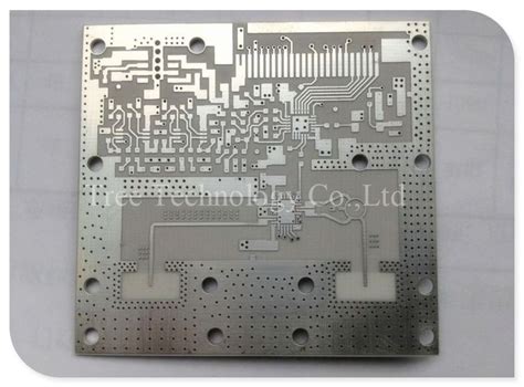
What is a PTH PCB?
A PTH PCB, or plated through-hole printed circuit board, is a type of PCB that features holes drilled through the board and electroplated with a conductive material, typically copper, to create electrical connections between the layers of the board. This process allows for the mounting of through-hole components and provides a robust mechanical and electrical connection.
PTH PCBs have been widely used in the electronics industry for decades due to their reliability and durability. They are commonly found in various applications, including:
- Consumer electronics
- Industrial equipment
- Automotive systems
- Medical devices
- Aerospace and defense applications
Advantages of PTH PCBs
PTH PCBs offer several advantages over other types of PCBs:
-
Mechanical Strength: The plated through-holes provide excellent mechanical strength and stability, making PTH PCBs ideal for applications that require high durability and resistance to vibration and shock.
-
Reliability: The electroplated through-holes ensure a reliable electrical connection between layers, reducing the risk of connection failures and improving the overall reliability of the circuit.
-
Ease of Assembly: Through-hole components are easier to install and replace compared to surface-mount components, making PTH PCBs a preferred choice for manual assembly and prototyping.
-
High Current Capacity: The plated through-holes can handle higher currents compared to the traces on the surface of the board, making PTH PCBs suitable for power electronics applications.
-
Thermal Management: The through-holes can also serve as thermal vias, helping to dissipate heat from high-power components and improving the thermal management of the circuit.

Manufacturing Process of PTH PCBs
The manufacturing process of PTH PCBs involves several steps:
-
Drilling: Holes are drilled through the PCB substrate at precise locations according to the design specifications.
-
Deburring: The drilled holes are deburred to remove any rough edges and ensure a smooth surface for plating.
-
Cleaning: The PCB is cleaned to remove any debris and contaminants that may interfere with the plating process.
-
Electroless Copper Deposition: A thin layer of copper is deposited onto the walls of the drilled holes and the surface of the PCB using an electroless plating process.
-
Electrolytic Copper Plating: The PCB is then subjected to an electrolytic plating process, which deposits a thicker layer of copper onto the walls of the holes and the surface of the board.
-
Resist Application: A photoresist material is applied to the surface of the PCB and patterned using photolithography to define the desired circuit layout.
-
Etching: The exposed copper is etched away, leaving behind the desired circuit pattern.
-
Resist Removal: The remaining photoresist is removed, revealing the final circuit pattern.
-
Solder Mask Application: A solder mask layer is applied to the surface of the PCB to protect the copper traces and prevent short circuits.
-
Surface Finish: A surface finish, such as HASL (Hot Air Solder Leveling) or ENIG (Electroless Nickel Immersion Gold), is applied to the exposed copper areas to improve solderability and protect against oxidation.

Design Considerations for PTH PCBs
When designing a PTH PCB, several factors must be considered to ensure optimal performance and manufacturability:
Hole Size and Spacing
The size and spacing of the drilled holes are critical factors in PTH PCB design. The hole size must be large enough to accommodate the leads of the through-hole components while maintaining sufficient space between holes to prevent electrical and mechanical interference. The minimum hole size and spacing are determined by the PCB manufacturing capabilities and the requirements of the specific application.
Typical hole sizes for PTH PCBs range from 0.3mm to 1.0mm, with a minimum spacing of 0.4mm to 0.8mm between holes. However, these values can vary depending on the PCB manufacturer and the specific design requirements.
Plating Thickness
The thickness of the copper plating in the through-holes is another crucial factor in PTH PCB design. The plating must be thick enough to provide a reliable electrical connection and withstand the mechanical stresses associated with component insertion and soldering.
The minimum plating thickness for PTH PCBs is typically 25μm (1 mil) for standard applications. However, for high-reliability applications or boards with high aspect ratio holes (depth-to-diameter ratio greater than 8:1), a thicker plating of 35μm to 50μm may be required.
Aspect Ratio
The aspect ratio of a plated through-hole is the ratio of its depth to its diameter. High aspect ratio holes can be challenging to plate uniformly, leading to issues such as incomplete plating or voids.
The maximum achievable aspect ratio depends on the PCB manufacturer’s capabilities and the specific plating process used. Generally, aspect ratios up to 8:1 can be reliably plated using standard processes, while higher aspect ratios may require specialized equipment and techniques.
Thermal Management
PTH PCBs can be designed to enhance thermal management by incorporating thermal vias. Thermal vias are plated through-holes that are strategically placed near high-power components to provide a low-resistance thermal path to the opposite side of the board or a dedicated heat sink.
When designing thermal vias, consider factors such as via size, spacing, and location to optimize heat dissipation while minimizing the impact on signal integrity and routing density.

PTH PCB Manufacturing Challenges and Solutions
Despite the advantages of PTH PCBs, there are several manufacturing challenges that must be addressed to ensure high-quality and reliable boards:
Hole Quality
Drilling precise and clean holes is essential for successful plating and component assembly. Common hole quality issues include:
- Roughness: Rough hole walls can lead to poor plating adhesion and increased resistance.
- Smear: Drilling can cause the epoxy resin in the PCB substrate to melt and smear onto the hole walls, insulating them and preventing proper plating.
- Burrs: Burrs around the hole edges can interfere with component insertion and soldering.
To mitigate these issues, manufacturers use high-quality drill bits, optimize drilling parameters, and employ proper deburring and cleaning techniques.
Plating Uniformity
Achieving uniform plating thickness in the through-holes is critical for reliable electrical connections. Plating uniformity can be affected by factors such as hole aspect ratio, plating chemistry, and current density.
Manufacturers use advanced plating processes, such as pulse plating or reverse pulse plating, to improve plating uniformity in high aspect ratio holes. They also carefully control the plating chemistry and current density to ensure consistent results.
Solder wicking
Solder wicking, also known as capillary action, occurs when molten solder is drawn up into the plated through-holes during the soldering process. This can lead to insufficient solder on the component leads and potentially weaken the mechanical and electrical connection.
To prevent solder wicking, manufacturers can use solder masks to cover the annular rings around the holes or apply a solder resist material inside the holes. Additionally, proper control of soldering temperature and duration can help minimize solder wicking.
Comparison of PTH and SMT PCBs
While PTH PCBs have been the traditional choice for many applications, surface-mount technology (SMT) has gained popularity in recent years due to its advantages in miniaturization and high-density packaging. Here’s a comparison of PTH and SMT PCBs:
| Feature | PTH PCB | SMT PCB |
|---|---|---|
| Component Mounting | Through-hole components | Surface-mount components |
| Board Density | Lower component density | Higher component density |
| Assembly Process | Manual or wave soldering | Automated pick-and-place and reflow soldering |
| Mechanical Strength | High, suitable for harsh environments | Lower, more susceptible to vibration and shock |
| Thermal Management | Through-holes can serve as thermal vias | Limited thermal management options |
| Repair and Rework | Easier to repair and replace components | More challenging to repair and rework |
| Cost | Higher for low-volume production | Lower for high-volume production |
| Size and Weight | Larger and heavier | Smaller and lighter |
In practice, many modern PCBs use a combination of PTH and SMT technologies to leverage the benefits of both. For example, a board may use SMT for high-density digital circuits and PTH for power components or connectors that require greater mechanical strength.
Future Trends in PTH PCB Technology
As the electronics industry continues to evolve, PTH PCB technology is also adapting to meet new challenges and requirements:
-
High Aspect Ratio Plating: Advancements in plating technologies, such as conformal plating or advanced electrolytic plating, are enabling the reliable plating of through-holes with aspect ratios up to 20:1. This allows for the development of more compact and high-density PCBs.
-
Embedded Components: PTH PCBs can be designed with embedded components, such as resistors or capacitors, which are placed inside the board substrate rather than on the surface. This technique can save space, reduce parasitic effects, and improve overall circuit performance.
-
3D PCBs: The use of 3D printing technologies in PCB manufacturing is opening up new possibilities for PTH PCBs. 3D-printed PCBs can have complex geometries and non-planar surfaces, enabling the creation of innovative and space-saving designs.
-
Advanced Materials: The development of new PCB substrate materials, such as high-frequency laminates or thermally conductive materials, is expanding the application range of PTH PCBs in demanding environments, such as 5G telecommunications or high-power electronics.
As these trends continue to shape the future of PTH PCB technology, designers and manufacturers must stay informed and adapt their practices to take full advantage of the latest advancements.
Frequently Asked Questions (FAQ)
-
What is the difference between a PTH PCB and a non-PTH PCB?
A PTH PCB has plated through-holes that provide electrical connections between layers and allow for the mounting of through-hole components. A non-PTH PCB, also known as a surface-mount PCB, does not have plated through-holes and relies on surface-mount components and conductive traces on the surface of the board for electrical connections. -
Can PTH PCBs be used for high-frequency applications?
While PTH PCBs can be used for high-frequency applications, they may face some limitations compared to surface-mount PCBs. The through-holes can introduce parasitic capacitance and inductance, which can affect signal integrity at high frequencies. However, with proper design techniques and the use of advanced materials, PTH PCBs can still be viable for many high-frequency applications. -
Are PTH PCBs more expensive than SMT PCBs?
The cost of PTH PCBs compared to SMT PCBs depends on factors such as board complexity, volume, and manufacturing process. In general, PTH PCBs tend to be more expensive for low-volume production due to the additional drilling and plating steps. However, for high-volume production, the cost difference between PTH and SMT PCBs may be less significant. -
How do I choose between a PTH PCB and an SMT PCB for my application?
The choice between a PTH PCB and an SMT PCB depends on several factors, including: - Component availability and packaging
- Required board density and size
- Mechanical strength and durability requirements
- Thermal management needs
-
Manufacturing volume and cost constraints
Consider these factors and consult with a PCB manufacturer or design expert to determine the best option for your specific application. -
Can PTH and SMT components be used together on the same PCB?
Yes, it is common to use both PTH and SMT components on the same PCB. This hybrid approach allows designers to leverage the benefits of both technologies, such as using PTH for connectors and power components while using SMT for high-density digital circuits. However, the design and manufacturing process must account for the specific requirements of each component type to ensure compatibility and reliability.


Leave a Reply