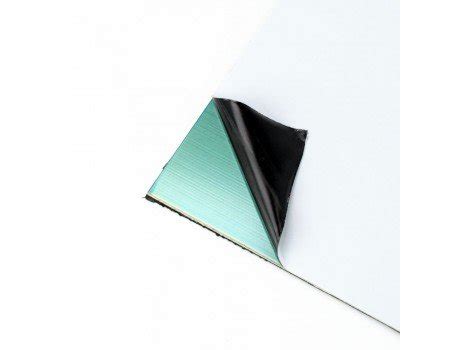
What is a Presensitized PCB?
Presensitized PCB, also known as photosensitive PCB or pre-coated PCB, is a type of printed circuit board that comes with a light-sensitive photoresist layer pre-applied to the copper surface. This photoresist layer is essential for creating the desired circuit pattern on the board through a process called photolithography.
Advantages of Presensitized PCBs
Presensitized PCBs offer several advantages over conventional PCBs, including:
- Simplified manufacturing process
- Improved accuracy and precision
- Faster turnaround times
- Reduced material waste
- Enhanced circuit complexity
How are Presensitized PCBs Manufactured?
The manufacturing process of presensitized PCBs involves several key steps:
1. Substrate Preparation
The PCB substrate, typically made of fiberglass or epoxy, is cleaned and treated to ensure proper adhesion of the copper layer.
2. Copper Lamination
A thin layer of copper foil is laminated onto the substrate using heat and pressure.
3. Photoresist Application
The presensitized photoresist layer is applied evenly across the copper surface using a specialized coating machine.
4. Exposure and Development
The desired circuit pattern is transferred onto the photoresist layer using a photomask and UV light exposure. The exposed areas of the photoresist are then removed using a chemical developer, revealing the underlying copper.
5. Etching
The exposed copper is etched away using a chemical solution, leaving only the desired circuit pattern.
6. Photoresist Removal
The remaining photoresist is stripped off using a chemical solvent, revealing the final copper circuit pattern.
7. Surface Finishing
Additional surface treatments, such as solder mask application and silkscreen printing, are applied to protect the circuit and improve its functionality.
Types of Photoresist Used in Presensitized PCBs
There are two main types of photoresist used in presensitized PCBs:
- Positive Photoresist
- Exposed areas become soluble and are removed during development
-
Resulting circuit pattern matches the photomask design
-
Negative Photoresist
- Exposed areas become insoluble and remain after development
- Resulting circuit pattern is the inverse of the photomask design
The choice of photoresist depends on the specific requirements of the PCB design and manufacturing process.

Photolithography in Presensitized PCB Manufacturing
Photolithography is a critical step in the manufacturing of presensitized PCBs. It involves the following key components:
1. Photomask
A photomask is a transparent sheet with opaque areas that define the desired circuit pattern. It is used to selectively expose the photoresist layer to UV light.
2. UV Light Exposure
The presensitized PCB is placed under a UV light source, with the photomask positioned between the light source and the board. The UV light passes through the transparent areas of the photomask, exposing the corresponding areas of the photoresist.
3. Development
After exposure, the PCB is immersed in a chemical developer solution. For positive photoresist, the exposed areas become soluble and are removed, while for negative photoresist, the unexposed areas are removed.
Advantages of Photolithography in PCB Manufacturing
Photolithography offers several advantages in PCB manufacturing, including:
- High resolution and accuracy
- Ability to create complex circuit patterns
- Scalability for high-volume production
- Compatibility with a wide range of substrate materials
Challenges and Considerations in Presensitized PCB Manufacturing
While presensitized PCBs offer many benefits, there are also some challenges and considerations to keep in mind:
- Proper handling and storage of photoresist-coated boards
- Accurate alignment of photomask and PCB during exposure
- Control of exposure time and intensity
- Chemical safety and waste management during development and etching
- Compatibility of photoresist with desired surface finishes and soldermask
Applications of Presensitized PCBs
Presensitized PCBs are widely used in various industries and applications, including:
- Consumer electronics
- Automotive electronics
- Medical devices
- Telecommunications equipment
- Aerospace and defense systems
The high precision and reliability offered by presensitized PCBs make them ideal for applications that require complex circuit designs and strict performance requirements.
Frequently Asked Questions (FAQ)
1. What is the shelf life of presensitized PCBs?
The shelf life of presensitized PCBs depends on the specific photoresist used and the storage conditions. Typically, presensitized PCBs have a shelf life of 6-12 months when stored in a cool, dry, and dark environment.
2. Can presensitized PCBs be reworked or repaired?
Reworking or repairing presensitized PCBs can be challenging due to the presence of the photoresist layer. In most cases, it is recommended to manufacture a new PCB rather than attempting to rework or repair a presensitized board.
3. How do I select the appropriate photoresist for my PCB design?
The choice of photoresist depends on factors such as the desired circuit feature size, substrate material, and processing conditions. Consult with your PCB manufacturer or photoresist supplier to determine the most suitable option for your specific application.
4. Can presensitized PCBs be used for multi-layer designs?
Yes, presensitized PCBs can be used for multi-layer designs. The photolithography process is repeated for each layer, with careful alignment and registration to ensure proper interconnections between layers.
5. Are there any environmental concerns associated with presensitized PCB manufacturing?
The chemicals used in the photolithography and Etching Processes can pose environmental concerns if not handled and disposed of properly. PCB Manufacturers must follow strict regulations and guidelines for chemical safety and waste management to minimize environmental impact.
Conclusion
Presensitized PCBs offer a reliable and efficient solution for creating high-quality printed circuit boards with complex designs. By leveraging the power of photolithography, presensitized PCBs enable faster turnaround times, improved accuracy, and greater design flexibility compared to traditional PCB manufacturing methods.
As the electronics industry continues to evolve and demand more advanced circuit designs, presensitized PCBs will play an increasingly important role in enabling the next generation of electronic devices and systems.


Leave a Reply