Introduction to PCB Decoupling
Printed Circuit Board (PCB) design is a complex process that involves various aspects, including component placement, signal integrity, and power supply management. One crucial aspect of PCB design is power supply noise decoupling, which ensures that the electronic components receive a clean and stable power supply. In this article, we will delve into the concept of PCB decoupling, its importance, and the techniques used to achieve effective power supply noise reduction.
What is PCB Decoupling?
PCB decoupling is the process of reducing high-frequency noise and voltage fluctuations in the power supply lines of a PCB. This is achieved by strategically placing decoupling capacitors near the power pins of integrated circuits (ICs) and other components. Decoupling capacitors act as local energy reservoirs, providing a low-impedance path for high-frequency noise and preventing it from propagating throughout the power supply network.
Why is PCB Decoupling Important?
Effective PCB decoupling is essential for several reasons:
-
Noise Reduction: Decoupling capacitors help to filter out high-frequency noise generated by digital circuits, such as microprocessors and FPGAs. This noise can cause signal integrity issues and lead to system instability or malfunctions.
-
Power Supply Stability: Decoupling capacitors provide a stable and clean power supply to the electronic components. They minimize voltage fluctuations caused by sudden changes in current demand, ensuring that the components receive the required voltage levels for proper operation.
-
EMI Reduction: By reducing high-frequency noise, decoupling capacitors also help to minimize electromagnetic interference (EMI) emanating from the PCB. This is important for meeting EMC (electromagnetic compatibility) regulations and preventing interference with other electronic devices.
-
Improved Signal Integrity: Clean power supply lines contribute to better signal integrity by reducing crosstalk and other noise-related issues. This is particularly important for high-speed digital circuits and analog circuits sensitive to noise.
Decoupling Capacitor Selection and Placement
Types of Decoupling Capacitors
There are several types of decoupling capacitors commonly used in PCB design:
-
Ceramic Capacitors: Ceramic capacitors, particularly multilayer ceramic capacitors (MLCCs), are the most widely used type for decoupling. They offer low equivalent series resistance (ESR), low equivalent series inductance (ESL), and high capacitance values in small package sizes.
-
Tantalum Capacitors: Tantalum capacitors provide high capacitance values and are suitable for low-frequency decoupling. However, they have higher ESR compared to ceramic capacitors and are more prone to failure under certain conditions.
-
Electrolytic Capacitors: Electrolytic capacitors, such as aluminum electrolytic capacitors, offer high capacitance values but have higher ESR and larger package sizes compared to ceramic capacitors. They are commonly used for bulk decoupling on power supply lines.
Selecting the Right Capacitance Value
Choosing the appropriate capacitance value for decoupling capacitors depends on several factors:
-
Frequency Range: The capacitance value should be selected based on the frequency range of the noise to be filtered. Higher capacitance values are effective for lower frequencies, while lower capacitance values are suitable for higher frequencies.
-
Current Requirements: The capacitance value should be sufficient to supply the required current to the components during transient events, such as switching loads or signal transitions.
-
Resonance Frequency: The combination of capacitance and inductance in the decoupling network forms a resonant circuit. The resonance frequency should be chosen to avoid amplifying noise at specific frequencies.
A common approach is to use a combination of capacitors with different values to cover a wide frequency range. For example, using a larger bulk capacitor (e.g., 10 µF) for low-frequency decoupling and smaller capacitors (e.g., 0.1 µF, 0.01 µF) for high-frequency decoupling.
Placement of Decoupling Capacitors
The placement of decoupling capacitors on the PCB is critical for their effectiveness. Here are some guidelines for capacitor placement:
-
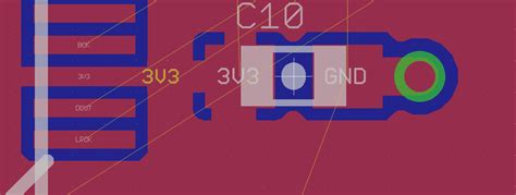
Proximity to Power Pins: Decoupling capacitors should be placed as close as possible to the power pins of the ICs they are decoupling. This minimizes the inductance in the connection and provides a low-impedance path for noise.
-
Minimizing Loop Area: The loop area formed by the capacitor and the power/ground planes should be minimized to reduce inductance. This can be achieved by placing the capacitor on the same layer as the power plane and using short, wide traces.
-
Distributed Decoupling: Instead of relying on a single large capacitor, it is often more effective to distribute multiple smaller capacitors across the PCB. This helps to localize the decoupling and reduces the overall impedance of the power distribution network.
-
Placement on Power Planes: Decoupling capacitors should be placed directly on the power and ground planes to minimize the inductance in the connection. Via-in-pad or micro-via techniques can be used to achieve this.

Power and Ground Plane Design
Power and Ground Plane Partitioning
Proper partitioning of power and ground planes is essential for effective decoupling and noise reduction. Here are some considerations for plane partitioning:
-
Separate Analog and Digital Planes: It is recommended to use separate power and ground planes for analog and digital circuits to minimize noise coupling between them. This helps to isolate sensitive analog circuits from noisy digital circuits.
-
Split Planes for Different Voltages: If the PCB design includes multiple voltage levels, it is advisable to use split planes for each voltage. This allows for better control over power distribution and decoupling for each voltage domain.
-
Avoid Splitting Ground Planes: Splitting ground planes should be avoided whenever possible. A continuous ground plane provides a low-impedance return path for currents and helps to minimize ground bounce and other noise-related issues.
Power and Ground Plane Copper Pour
Copper pour on power and ground planes plays a crucial role in power supply noise reduction. Here are some guidelines for copper pour:
-
Maximize Copper Coverage: Increasing the copper coverage on power and ground planes helps to lower the impedance and improve noise reduction. This can be achieved by using wider traces and filling unused areas with copper.
-
Maintain Uniform Copper Distribution: Ensure that the copper distribution on the planes is uniform to avoid current crowding and voltage gradients. Use hatched or cross-hatched fills to maintain uniform copper density.
-
Avoid Large Gaps: Minimize large gaps or slots in the power and ground planes, as they can increase impedance and create discontinuities. If gaps are unavoidable, use stitching capacitors or copper bridges to maintain continuity.

Decoupling Techniques for High-Speed Designs
High-Frequency Decoupling
High-speed digital circuits, such as microprocessors and FPGAs, require special attention to decoupling at high frequencies. Here are some techniques for high-frequency decoupling:
-
Use of Low-ESL Capacitors: Capacitors with low equivalent series inductance (ESL) are essential for high-frequency decoupling. MLCCs with small package sizes, such as 0201 or 01005, are commonly used for this purpose.
-
Placement of Decoupling Capacitors: For high-speed designs, decoupling capacitors should be placed as close as possible to the power pins of the ICs. The use of via-in-pad or micro-via techniques can help to minimize the inductance in the connection.
-
Multiple Decoupling Stages: Implementing multiple stages of decoupling, with different capacitor values and placement, can help to cover a wide frequency range and provide effective noise reduction.
Power Plane Resonance and Mitigation
Power plane resonance is a common issue in high-speed designs, where the power and ground planes form a cavity resonator. This can lead to increased noise and signal integrity issues. Here are some techniques to mitigate power plane resonance:
-
Spreading Capacitors: Spreading decoupling capacitors across the PCB, rather than concentrating them in a single area, can help to dampen power plane resonance. This distributes the decoupling effect and reduces the impact of resonance.
-
Use of Embedded Capacitance: Embedded capacitance techniques, such as using high-k dielectric materials or power/ground plane pairs, can help to mitigate power plane resonance by providing distributed decoupling.
-
Stitching Capacitors: Placing stitching capacitors at the edges of the power planes can help to dampen resonance and reduce noise coupling between planes.

Simulation and Analysis
Power Integrity Simulation
Power integrity simulation is an essential tool for evaluating the effectiveness of decoupling strategies and identifying potential issues. Here are some aspects of power integrity simulation:
-
Impedance Analysis: Simulating the impedance profile of the power distribution network helps to identify resonance frequencies and areas of high impedance. This information can be used to optimize the decoupling network and placement of capacitors.
-
Transient Analysis: Transient simulations help to analyze the voltage fluctuations and noise on the power supply lines during switching events or load changes. This allows for the assessment of decoupling capacitor performance and the identification of voltage droop or overshoot issues.
-
Power Plane Resonance Analysis: Simulating power plane resonance helps to identify problematic frequencies and evaluate the effectiveness of mitigation techniques, such as spreading capacitors or using stitching capacitors.
Electromagnetic Simulation
Electromagnetic simulation tools, such as 3D full-wave solvers, can provide valuable insights into the electromagnetic behavior of the PCB. These simulations help to analyze the following aspects:
-
Impedance Discontinuities: Identifying impedance discontinuities in the power distribution network, such as vias or plane transitions, can help to optimize the design and minimize reflections.
-
Electromagnetic Coupling: Simulating electromagnetic coupling between power/ground planes and signal traces can help to identify potential crosstalk and EMI issues.
-
Radiation Analysis: Electromagnetic simulations can also be used to analyze the radiation characteristics of the PCB and evaluate the effectiveness of EMI reduction techniques, such as shielding or grounding.
Measuring and Testing
Power Supply Noise Measurement
Measuring power supply noise is crucial for validating the effectiveness of decoupling techniques and ensuring that the noise levels are within acceptable limits. Here are some methods for power supply noise measurement:
-
Oscilloscope Measurements: Using an oscilloscope to measure the voltage ripple and noise on the power supply lines provides a direct view of the noise waveform. High-bandwidth oscilloscopes and low-inductance probes are recommended for accurate measurements.
-
Spectrum Analyzer Measurements: Spectrum analyzers can be used to measure the frequency spectrum of the power supply noise. This helps to identify dominant noise frequencies and evaluate the effectiveness of decoupling capacitors at different frequencies.
-
Noise Injection Testing: Injecting controlled noise signals into the power supply lines and measuring the response can help to characterize the effectiveness of the decoupling network and identify potential weaknesses.
Decoupling Network Impedance Measurement
Measuring the impedance of the decoupling network is important for verifying the design and identifying any issues. Here are some methods for impedance measurement:
-
Vector Network Analyzer (VNA) Measurements: A VNA can be used to measure the impedance of the decoupling network over a wide frequency range. This provides valuable information about the effectiveness of the decoupling capacitors and the presence of resonance peaks.
-
Time Domain Reflectometry (TDR) Measurements: TDR Measurements can be used to characterize the impedance profile of the power distribution network in the time domain. This helps to identify impedance discontinuities and reflections.
Best Practices and Guidelines
Design for Manufacturability (DFM)
When designing the decoupling network, it is important to consider manufacturability aspects to ensure reliable and cost-effective production. Here are some DFM guidelines:
-
Component Selection: Choose decoupling capacitors that are readily available and have standard package sizes. Avoid using obsolete or hard-to-source components.
-
Placement and Routing: Ensure that the placement and routing of decoupling capacitors are compatible with the manufacturing process. Consider the clearance requirements and routing constraints of the PCB Fabrication and assembly processes.
-
Testability: Design the decoupling network in a way that facilitates testing and inspection. Provide test points or probe pads for measuring power supply noise and verifying the functionality of the decoupling capacitors.
Collaborative Design Approach
Effective power supply noise decoupling requires a collaborative approach involving different disciplines, such as PCB layout, signal integrity, and power integrity. Here are some recommendations for a collaborative design approach:
-
Early Collaboration: Engage all relevant stakeholders, including PCB designers, signal integrity engineers, and power integrity specialists, early in the design process. This allows for the identification of potential issues and the development of a comprehensive decoupling strategy.
-
Iterative Design Process: Follow an iterative design process that involves simulation, analysis, and feedback loops. This enables the refinement of the decoupling network based on simulation results and measurements.
-
Documentation and Communication: Maintain clear documentation of the decoupling strategy, including component selection, placement guidelines, and simulation results. Ensure effective communication among team members to align design goals and constraints.
Conclusion
Power supply noise decoupling is a critical aspect of PCB design that ensures the integrity and stability of the power supply network. Effective decoupling techniques, such as proper capacitor selection and placement, power and ground plane design, and high-frequency decoupling strategies, help to reduce noise, improve signal integrity, and minimize EMI.
By following best practices, such as considering manufacturability aspects and adopting a collaborative design approach, designers can develop robust and reliable decoupling solutions. Simulation and measurement techniques provide valuable insights into the performance of the decoupling network and help to validate the design.
Investing time and effort into proper power supply noise decoupling pays off in terms of improved system performance, reduced debugging time, and enhanced product reliability. As PCB designs continue to push the boundaries of speed and complexity, effective decoupling techniques will remain essential for ensuring the success of electronic products.
Frequently Asked Questions (FAQ)
-
What is the purpose of decoupling capacitors in PCB design?
Decoupling capacitors serve to reduce high-frequency noise and voltage fluctuations on the power supply lines of a PCB. They provide a local energy reservoir and a low-impedance path for noise, preventing it from propagating throughout the power supply network. -
How do I select the right capacitance value for decoupling capacitors?
The selection of capacitance value depends on factors such as the frequency range of the noise to be filtered, the current requirements of the components, and the desired resonance frequency. A common approach is to use a combination of capacitors with different values to cover a wide frequency range, such as a larger bulk capacitor for low frequencies and smaller capacitors for high frequencies. -
Where should decoupling capacitors be placed on the PCB?
Decoupling capacitors should be placed as close as possible to the power pins of the ICs they are decoupling. This minimizes the inductance in the connection and provides a low-impedance path for noise. The loop area formed by the capacitor and the power/ground planes should also be minimized to reduce inductance. -
What are the considerations for power and ground plane design in relation to decoupling?
Proper partitioning of power and ground planes is important for effective decoupling. It is recommended to use separate planes for analog and digital circuits, split planes for different voltage levels, and avoid splitting ground planes. Maximizing copper coverage and maintaining uniform copper distribution on the planes helps to lower impedance and improve noise reduction. -
How can I measure and validate the effectiveness of my decoupling network?
Power supply noise can be measured using oscilloscopes to observe voltage ripple and noise waveforms, spectrum analyzers to analyze the frequency spectrum of the noise, and noise injection testing to characterize the decoupling network’s response. The impedance of the decoupling network can be measured using vector network analyzers (VNA) or time-domain reflectometry (TDR) techniques to verify the design and identify any issues.
| Component | Frequency Range | Typical Capacitance Values |
|---|---|---|
| Bulk Capacitor | Low Frequency | 10 µF – 100 µF |
| Ceramic Capacitor | High Frequency | 0.01 µF – 1 µF |
| Tantalum Capacitor | Low Frequency | 1 µF – 100 µF |
Table: Common Decoupling Capacitor Types and Typical Values
| Technique | Purpose |
|---|---|
| Power Plane Partitioning | Isolate analog and digital circuits |
| Split Planes | Control power distribution for different voltages |
| Copper Pour | Lower impedance and improve noise reduction |
| Via-in-Pad Placement | Minimize inductance in capacitor connection |
| Stitching Capacitors | Dampen power plane resonance and reduce noise |
Table: Decoupling Techniques and Their Purposes
By understanding and applying the concepts


Leave a Reply