Understanding PCB Thickness
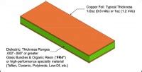
PCB thickness is typically measured in either millimeters (mm) or mils (thousands of an inch). The most common PCB thickness options range from 0.4mm to 3.2mm, with 1.6mm being the most widely used standard. The choice of PCB thickness depends on various factors, such as the application, component requirements, and manufacturing constraints.
Common PCB Thickness Options
| Thickness (mm) | Thickness (mils) | Common Applications |
|---|---|---|
| 0.4 | 15.75 | Flexible PCBs, wearable devices |
| 0.6 | 23.62 | High-density designs, mobile devices |
| 0.8 | 31.50 | Compact electronics, IoT devices |
| 1.0 | 39.37 | General-purpose electronics, consumer products |
| 1.2 | 47.24 | Automotive electronics, industrial control systems |
| 1.6 | 62.99 | Most common standard, suitable for various applications |
| 2.0 | 78.74 | Power electronics, high-current applications |
| 2.4 | 94.49 | Heavy-duty industrial equipment, aerospace applications |
| 3.2 | 125.98 | Extreme environments, military-grade electronics |
Factors Influencing PCB Thickness Selection
When choosing the appropriate PCB thickness for your project, consider the following factors:
1. Application Requirements
The intended application of your PCB plays a significant role in determining the appropriate thickness. For example, flexible PCBs used in wearable devices may require a thinner profile (0.4mm or 0.6mm) to ensure flexibility and comfort. On the other hand, power electronics handling high currents may demand thicker boards (2.0mm or above) to accommodate larger copper traces and improve heat dissipation.
2. Component Placement and Density
The size and density of components on your PCB can influence the choice of thickness. High-density designs with small components, such as those found in mobile devices, may benefit from thinner boards (0.6mm or 0.8mm) to minimize the overall device thickness. However, if your design includes larger or heavier components, a thicker board (1.6mm or above) may be necessary to provide adequate support and prevent warping.
3. Manufacturing Constraints
PCB manufacturing capabilities and constraints should also be taken into account when selecting the thickness. Some manufacturers may have limitations on the minimum or maximum thickness they can produce reliably. Additionally, thinner boards (below 0.8mm) may require specialized manufacturing processes and handling, which can increase production costs and lead times.
4. Mechanical Strength and Durability
The mechanical strength and durability of your PCB are directly related to its thickness. Thicker boards offer better resistance to bending, twisting, and impact forces, making them suitable for applications exposed to harsh environments or mechanical stress. If your PCB needs to withstand vibrations, shocks, or extreme temperatures, consider using a thicker board (1.6mm or above) to ensure long-term reliability.
5. Signal Integrity and Impedance Control
For high-speed digital circuits or RF applications, signal integrity and impedance control are critical considerations. The thickness of the PCB can affect the characteristic impedance of the traces and the overall signal quality. Thinner boards (0.8mm or below) may be preferred for high-speed designs to minimize signal reflections and maintain consistent impedance. However, the specific requirements may vary depending on the operating frequency and the desired impedance values.

PCB Thickness and Layer Count
In addition to the overall thickness, the number of layers in a PCB also plays a role in determining the appropriate thickness. As the layer count increases, the PCB thickness typically needs to increase as well to accommodate the additional copper layers and insulation materials.
| Layer Count | Typical Thickness Range (mm) |
|---|---|
| 1-2 | 0.4 – 1.0 |
| 4 | 1.0 – 1.6 |
| 6 | 1.2 – 2.0 |
| 8 | 1.6 – 2.4 |
| 10+ | 2.0 – 3.2+ |
It’s important to note that these are general guidelines, and the actual thickness requirements may vary based on the specific design and manufacturing constraints. Always consult with your PCB Manufacturer to determine the optimal thickness for your multi-layer PCB.

PCB Thickness and Cost Considerations
The choice of PCB thickness can also impact the overall cost of your project. Thinner boards (below 0.8mm) may require specialized manufacturing processes, which can increase production costs. On the other hand, thicker boards (above 2.0mm) may consume more raw materials and require longer drilling and plating times, also leading to higher costs.
When selecting the PCB thickness, it’s essential to strike a balance between the technical requirements and the cost implications. Consider the following cost-saving strategies:
- Use the standard 1.6mm thickness whenever possible, as it is widely available and offers a good balance between performance and cost.
- Minimize the number of layers in your PCB design to reduce the overall thickness and manufacturing complexity.
- Optimize your component placement and routing to minimize the required board size and thickness.
- Consult with your PCB manufacturer early in the design process to identify cost-effective thickness options that meet your requirements.

Frequently Asked Questions (FAQ)
1. What is the most common PCB thickness?
The most common PCB thickness is 1.6mm (62.99 mils). This thickness is widely used across various applications and offers a good balance between mechanical strength, manufacturability, and cost.
2. Can I use different thicknesses for different parts of my PCB?
Yes, it is possible to have different thicknesses within the same PCB, known as a “stepped” or “sculptured” design. This approach can be useful when you need to accommodate components with varying heights or when you require different thicknesses for specific sections of your board. However, stepped designs may increase manufacturing complexity and cost.
3. How does PCB thickness affect signal integrity?
PCB thickness can impact signal integrity, particularly in high-speed digital circuits or RF applications. Thinner boards may be preferred for these applications to minimize signal reflections and maintain consistent impedance. However, the specific requirements depend on factors such as the operating frequency, desired impedance values, and the overall design layout.
4. What is the minimum PCB thickness I can use?
The minimum PCB thickness depends on the manufacturing capabilities of your chosen PCB supplier. Some manufacturers can produce boards as thin as 0.4mm (15.75 mils) or even thinner for specialized applications like flexible PCBs. However, thinner boards may require specialized handling and processing, which can increase production costs and lead times.
5. How do I choose the right PCB thickness for my project?
To choose the right PCB thickness, consider factors such as the application requirements, component placement and density, manufacturing constraints, mechanical strength and durability, signal integrity, and cost implications. Consult with your PCB manufacturer early in the design process to discuss your specific needs and identify the most suitable thickness option for your project.
Conclusion
PCB thickness is a critical aspect of PCB design that impacts performance, durability, and manufacturing processes. The standard PCB thickness options range from 0.4mm to 3.2mm, with 1.6mm being the most common choice. When selecting the appropriate thickness for your project, consider factors such as the application requirements, component density, manufacturing constraints, mechanical strength, signal integrity, and cost implications.
By understanding the various PCB thickness options and their implications, you can make informed decisions that optimize your PCB design for performance, reliability, and cost-effectiveness. Always collaborate closely with your PCB manufacturer to ensure that your chosen thickness meets your specific requirements and is compatible with their manufacturing capabilities.


Leave a Reply