What are PCB Stencils?
PCB stencils, also known as solder paste stencils, are thin metal sheets with laser-cut openings that correspond to the pads on a PCB. They are used to apply solder paste to the PCB Pads in a precise and controlled manner. The stencil is placed over the PCB, and solder paste is spread across the surface using a squeegee or automated stencil printer. The solder paste is deposited through the openings onto the pads, creating a uniform layer ready for component placement.
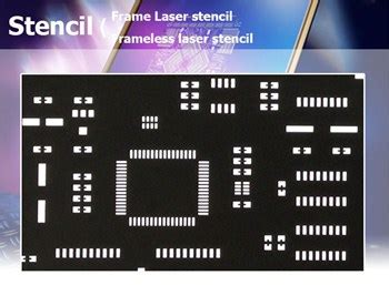
Types of PCB Stencils
There are two main types of PCB stencils:
- Framed Stencils
- Framed stencils have a metal frame surrounding the stencil, providing rigidity and ease of handling.
-
They are commonly used in manual stencil printing processes.
-
Frameless Stencils
- Frameless stencils consist of just the stencil material without a surrounding frame.
- They are typically used in automated stencil printing machines.
PCB Stencil Materials
PCB stencils can be made from various materials, each with its own characteristics and advantages:
| Material | Thickness | Durability | Cost |
|---|---|---|---|
| Stainless Steel | 0.1-0.2mm | High | High |
| Nickel | 0.1-0.15mm | Medium | Medium |
| Mylar (Polyester) | 0.1-0.13mm | Low | Low |
Stainless steel is the most common material for PCB stencils due to its durability and precision. Nickel stencils offer a balance between durability and cost, while Mylar stencils are a more affordable option for low-volume or prototype production.
How PCB Stencils Work
The process of using a PCB stencil involves the following steps:
-
Align the stencil: The stencil is carefully aligned with the PCB, ensuring that the openings match the pads on the board.
-
Apply solder paste: Solder paste is placed on one end of the stencil and spread across the surface using a squeegee or automated stencil printer. The solder paste is forced through the openings and onto the PCB PADS.
-
Remove the stencil: After the solder paste is applied, the stencil is carefully lifted off the PCB, leaving a precise amount of solder paste on each pad.
-
Place components: The PCB is now ready for component placement. The components are placed on the pads with the deposited solder paste.
-
Reflow soldering: The PCB undergoes a reflow soldering process, where it is heated in a controlled manner to melt the solder paste and create a strong bond between the components and the PCB pads.
Advantages of Using PCB Stencils
Using PCB stencils offers several advantages over manual solder paste application methods:
-
Precision: Stencils ensure precise and consistent solder paste deposition, resulting in uniform solder joints and improved reliability.
-
Efficiency: Stencil printing is a fast and efficient process, especially when using automated stencil printers, enabling high-volume production.
-
Repeatability: Stencils provide repeatable results, ensuring consistency across multiple PCBs in a production run.
-
Cost-effectiveness: While the initial cost of a stencil may be higher than manual methods, the improved efficiency and quality justify the investment, particularly for larger production volumes.

How to Make PCB Stencils
Making your own PCB stencils involves several steps and considerations. Let’s explore the process in detail:
Step 1: Prepare the PCB Design
Start by creating or obtaining the PCB design files, usually in Gerber format. Ensure that the design includes the necessary pad information for stencil creation.
Step 2: Choose the Stencil Material
Select the appropriate stencil material based on your requirements. Stainless steel is the most common choice for its durability and precision.
Step 3: Determine the Stencil Thickness
The stencil thickness depends on the solder paste and PCB Requirements. Typical thicknesses range from 0.1mm to 0.2mm. Consult the solder paste manufacturer’s recommendations for the appropriate thickness.
Step 4: Create the Stencil Artwork
Use PCB design software or a dedicated stencil design tool to create the stencil artwork. The artwork should include the openings for the pads, as well as any necessary fiducial marks or alignment features.
Step 5: Generate the Stencil File
Export the stencil artwork as a vector file, such as DXF or Gerber. This file will be used by the stencil manufacturer to create the physical stencil.
Step 6: Choose a Stencil Manufacturer
Research and select a reputable stencil manufacturer. Consider factors such as quality, turnaround time, pricing, and customer support.
Step 7: Send the Stencil File for Manufacturing
Provide the stencil manufacturer with the stencil file, specifying the material, thickness, and any additional requirements. The manufacturer will use laser cutting or chemical etching to create the stencil according to your specifications.
Step 8: Inspect and Test the Stencil
Upon receiving the manufactured stencil, carefully inspect it for any defects or inconsistencies. Test the stencil by aligning it with a PCB and applying solder paste to ensure proper fit and paste deposition.

Tips for Successful PCB Stencil Usage
To get the best results from your PCB stencils, consider the following tips:
-
Proper alignment: Ensure precise alignment between the stencil and the PCB to avoid misaligned solder paste deposition.
-
Solder paste selection: Choose a solder paste that is compatible with your PCB and stencil, considering factors such as particle size, viscosity, and printing requirements.
-
Squeegee pressure and speed: Apply the appropriate pressure and speed when spreading the solder paste across the stencil to achieve optimal paste deposition.
-
Stencil cleaning: Regularly clean the stencil to prevent solder paste buildup and ensure consistent printing results. Use a compatible cleaning solution and follow the manufacturer’s recommendations.
-
Storage and handling: Store the stencil in a clean, dry environment to prevent damage or contamination. Handle the stencil with care to avoid bending or warping.

Frequently Asked Questions (FAQ)
1. Can I reuse a PCB stencil?
Yes, PCB stencils can be reused multiple times if properly cleaned and maintained. However, over time, the stencil may experience wear and tear, affecting its performance. It’s important to regularly inspect the stencil for any signs of damage or degradation.
2. How do I clean a PCB stencil?
To clean a PCB stencil, use a compatible cleaning solution specifically designed for solder paste residue. Apply the solution to the stencil and use a soft brush or lint-free cloth to gently scrub the surface. Rinse the stencil with isopropyl alcohol or deionized water and dry it thoroughly before storing.
3. What is the typical lifespan of a PCB stencil?
The lifespan of a PCB stencil depends on various factors, such as the material, usage frequency, and maintenance. Stainless steel stencils can last for thousands of prints if properly cared for, while Mylar stencils have a shorter lifespan. Regular inspection and timely replacement can help ensure optimal performance.
4. How do I store PCB stencils?
Store PCB stencils in a clean, dry environment, preferably in a dedicated storage container or rack. Avoid exposing the stencils to extreme temperatures, humidity, or direct sunlight. If storing multiple stencils together, use separators to prevent them from contacting each other and potentially causing damage.
5. Can I make my own PCB stencils at home?
While it is possible to make PCB stencils at home using materials like Mylar or vinyl, the process can be challenging and may not yield the same level of precision and durability as professionally manufactured stencils. For best results, it is recommended to use a reputable stencil manufacturer with the necessary equipment and expertise.
Conclusion
PCB stencils are a crucial tool for achieving precise and efficient solder paste application in PCB Assembly. By understanding the types, materials, and process of using PCB stencils, you can greatly improve the quality and consistency of your soldering results. Making your own PCB stencils involves careful design, material selection, and collaboration with a reliable stencil manufacturer.
By following the steps outlined in this guide and considering the tips for successful usage, you can create and utilize PCB stencils effectively in your PCB assembly workflow. Whether you are a hobbyist or a professional, investing in high-quality PCB stencils can significantly enhance your PCB manufacturing capabilities and outcomes.


Leave a Reply