What is PCB Stackup?
PCB stackup refers to the arrangement of layers in a printed circuit board (PCB). It is a critical aspect of PCB design that determines the board’s electrical performance, signal integrity, and manufacturability. A well-planned PCB stackup ensures that the board functions as intended and meets the required specifications.
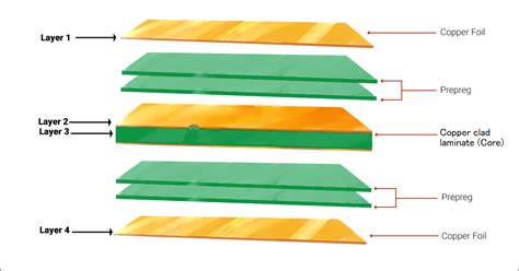
Key Components of a PCB Stackup
A typical PCB stackup consists of the following components:
- Copper layers: These are the conductive layers that carry electrical signals and power.
- Dielectric layers: These are the insulating layers that separate the copper layers and provide mechanical support.
- Solder Mask: This is a protective coating applied to the outer layers of the PCB to prevent short circuits and improve solderability.
- Silkscreen: This is a layer of text and symbols printed on the PCB for identification and assembly purposes.
Importance of PCB Stackup Planning
Proper PCB stackup planning is essential for several reasons:
- Signal integrity: A well-designed stackup ensures that signals travel through the board with minimal distortion, crosstalk, and electromagnetic interference (EMI).
- Power integrity: The stackup must provide adequate power distribution to all components on the board, minimizing voltage drop and ensuring stable power delivery.
- Manufacturability: The stackup must be compatible with the manufacturing processes and materials used by the PCB fabricator.
- Cost-effectiveness: An optimized stackup can reduce the number of layers required, lowering material and manufacturing costs.

Factors to Consider When Planning a PCB Stackup
When planning a PCB stackup, several factors must be taken into account:
1. Board Thickness
The overall thickness of the PCB is determined by the number of layers and the thickness of each layer. The board thickness must be compatible with the enclosure and other mechanical constraints of the product.
2. Layer Count
The number of layers in the stackup depends on the complexity of the circuit and the routing requirements. More layers provide more routing space but also increase the cost and complexity of the board.
3. Material Selection
The choice of materials for the dielectric and copper layers affects the electrical and mechanical properties of the board. Common dielectric materials include FR-4, Rogers, and Isola. Copper thickness is typically specified in ounces per square foot (oz/ft²).
4. Impedance Control
For high-speed designs, the stackup must be designed to maintain the desired characteristic impedance of the transmission lines. This requires careful selection of dielectric materials and thicknesses.
5. Via Technology
The type of vias used in the stackup affects the routing density and signal integrity of the board. Through-hole vias, blind vias, and buried vias each have their advantages and limitations.

Common PCB Stackup Configurations
There are several common PCB stackup configurations, each with its own advantages and applications:
1. 2-Layer Stackup
A 2-layer stackup is the simplest and most cost-effective configuration. It consists of two copper layers (top and bottom) separated by a single dielectric layer. This stackup is suitable for simple, low-density designs.
| Layer | Material | Thickness |
|---|---|---|
| Top Copper | 1 oz/ft² | 1.4 mil |
| FR-4 Core | – | 59.6 mil |
| Bottom Copper | 1 oz/ft² | 1.4 mil |
2. 4-Layer Stackup
A 4-layer stackup adds two internal copper layers to the 2-layer configuration. The internal layers are typically used for power and ground planes, providing a low-impedance path for power distribution and reducing EMI.
| Layer | Material | Thickness |
|---|---|---|
| Top Copper | 1 oz/ft² | 1.4 mil |
| FR-4 Prepreg | – | 6.7 mil |
| Inner Layer 1 (Ground) | 0.5 oz/ft² | 0.7 mil |
| FR-4 Core | – | 47.2 mil |
| Inner Layer 2 (Power) | 0.5 oz/ft² | 0.7 mil |
| FR-4 Prepreg | – | 6.7 mil |
| Bottom Copper | 1 oz/ft² | 1.4 mil |
3. 6-Layer Stackup
A 6-layer stackup adds two more internal layers to the 4-layer configuration. This provides additional routing space and allows for more complex signal routing and power distribution.
| Layer | Material | Thickness |
|---|---|---|
| Top Copper | 1 oz/ft² | 1.4 mil |
| FR-4 Prepreg | – | 6.7 mil |
| Inner Layer 1 (Signal) | 0.5 oz/ft² | 0.7 mil |
| FR-4 Core | – | 47.2 mil |
| Inner Layer 2 (Ground) | 0.5 oz/ft² | 0.7 mil |
| FR-4 Core | – | 47.2 mil |
| Inner Layer 3 (Power) | 0.5 oz/ft² | 0.7 mil |
| FR-4 Prepreg | – | 6.7 mil |
| Bottom Copper | 1 oz/ft² | 1.4 mil |
4. 8-Layer Stackup
An 8-layer stackup is used for high-density, high-speed designs that require extensive routing and power distribution. This stackup provides ample routing space and allows for sophisticated signal integrity techniques, such as differential pair routing and ground shielding.
| Layer | Material | Thickness |
|---|---|---|
| Top Copper | 1 oz/ft² | 1.4 mil |
| FR-4 Prepreg | – | 6.7 mil |
| Inner Layer 1 (Signal) | 0.5 oz/ft² | 0.7 mil |
| FR-4 Core | – | 47.2 mil |
| Inner Layer 2 (Ground) | 0.5 oz/ft² | 0.7 mil |
| FR-4 Core | – | 47.2 mil |
| Inner Layer 3 (Signal) | 0.5 oz/ft² | 0.7 mil |
| FR-4 Core | – | 47.2 mil |
| Inner Layer 4 (Power) | 0.5 oz/ft² | 0.7 mil |
| FR-4 Prepreg | – | 6.7 mil |
| Bottom Copper | 1 oz/ft² | 1.4 mil |

PCB Stackup Design Guidelines
To ensure a successful PCB stackup design, follow these guidelines:
- Keep the stackup symmetrical to minimize warpage and ensure even Copper Distribution.
- Use dedicated power and ground planes to provide low-impedance power distribution and reduce EMI.
- Route critical signals on inner layers to minimize crosstalk and external noise pickup.
- Use appropriate via technology to minimize signal integrity issues and improve routing density.
- Choose dielectric materials with suitable electrical properties for the desired frequency range and signal speeds.
- Maintain consistent dielectric thicknesses to ensure uniform impedance control.
- Adhere to the manufacturer’s design rules and guidelines for the chosen materials and processes.
PCB Stackup Documentation
Proper documentation of the PCB stackup is essential for communication between the design team and the manufacturer. A stackup diagram should include:
- Layer order and numbering
- Material specifications for each layer (Copper Weight, dielectric material, and thickness)
- Overall board thickness
- Impedance requirements (if applicable)
- Via types and sizes
- Special requirements (e.g., controlled depth drilling, back drilling)
Frequently Asked Questions (FAQ)
1. What is the most common PCB stackup?
The most common PCB stackup is the 4-layer configuration, which provides a good balance between routing space, power distribution, and cost. It is suitable for a wide range of applications, from simple to moderately complex designs.
2. How do I choose the right number of layers for my PCB stackup?
The number of layers in your PCB stackup depends on several factors, such as the complexity of the circuit, routing requirements, power distribution needs, and cost constraints. Start with the simplest stackup that meets your requirements and add layers as necessary.
3. What is the purpose of power and ground planes in a PCB stackup?
Power and ground planes serve several purposes in a PCB stackup:
- They provide a low-impedance path for power distribution, minimizing voltage drop and ensuring stable power delivery to components.
- They act as reference planes for signal layers, providing a constant reference voltage and reducing EMI.
- They help to control the impedance of the transmission lines on adjacent signal layers.
4. How does the choice of dielectric material affect my PCB stackup?
The choice of dielectric material affects the electrical and mechanical properties of your PCB stackup. Key properties to consider include:
- Dielectric constant (Dk): Affects the speed of signal propagation and the characteristic impedance of transmission lines.
- Dissipation factor (Df): Affects the signal loss and attenuation at high frequencies.
- Thermal expansion coefficient (CTE): Affects the board’s dimensional stability under temperature changes and the reliability of Plated Through-Holes.
Choose a dielectric material that provides the desired electrical performance and mechanical stability for your application.
5. What is the importance of stackup symmetry in PCB design?
Stackup symmetry is important in PCB design for several reasons:
- It helps to minimize warpage during the manufacturing process, ensuring a flat and dimensionally stable board.
- It ensures an even distribution of copper on both sides of the board, balancing the mechanical stresses and preventing delamination.
- It can help to cancel out the effects of thermal expansion, improving the board’s reliability under temperature changes.
To achieve stackup symmetry, arrange the layers so that the copper distribution is balanced around the center of the board, and use similar materials and thicknesses for layers equidistant from the center.
Conclusion
PCB stackup planning is a critical aspect of PCB design that directly impacts the board’s electrical performance, signal integrity, and manufacturability. By carefully considering factors such as board thickness, layer count, material selection, impedance control, and via technology, designers can create stackups that meet the required specifications and ensure reliable operation.
Common PCB stackup configurations, such as 2-layer, 4-layer, 6-layer, and 8-layer stackups, offer varying levels of complexity and performance, suitable for a wide range of applications. By following best practices and guidelines for PCB stackup design and documentation, designers can streamline the manufacturing process and achieve the desired results.
As PCB technology continues to evolve, with increasing demands for higher speeds, greater densities, and improved reliability, effective PCB stackup planning will remain a vital skill for electronics engineers and PCB designers.


Leave a Reply