Introduction to PCB SMT stencils
In the world of printed circuit board (PCB) manufacturing, surface mount technology (SMT) has become the dominant method for assembling electronic components onto PCBs. One crucial aspect of the SMT process is the application of solder paste onto the PCB pads. This is where PCB SMT stencils come into play, ensuring accurate and precise solder paste application for optimal component placement and soldering results.
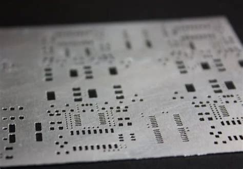
What is a PCB SMT Stencil?
A PCB SMT stencil is a thin, flat sheet of metal, usually made of stainless steel or nickel, with precisely cut openings that correspond to the pads on a PCB. The stencil is placed on top of the PCB, and solder paste is applied using a squeegee or automated solder paste printer. The openings in the stencil allow the solder paste to be deposited onto the pads in the correct amount and location.
Benefits of Using PCB SMT Stencils
Using PCB SMT stencils offers several benefits in the PCB assembly process:
- Accuracy: Stencils ensure that the solder paste is applied precisely where it’s needed, reducing the risk of bridging, solder balls, or insufficient solder joints.
- Consistency: With a stencil, the amount of solder paste applied to each pad is consistent, leading to more uniform solder joints and better overall PCB quality.
- Efficiency: Stencils enable faster solder paste application compared to manual methods, increasing production throughput and reducing assembly time.
- Cost-effectiveness: By minimizing solder paste waste and reducing rework due to soldering defects, stencils contribute to cost savings in the long run.
Types of PCB SMT Stencils
There are several types of PCB SMT stencils available, each with its own characteristics and applications.
Laser-Cut Stencils
Laser-cut stencils are created using a high-precision laser cutting machine. The laser beam vaporizes the stencil material, creating clean and accurate openings. Laser-cut stencils are suitable for fine-pitch components and high-density PCB designs.
Electroformed Stencils
Electroformed stencils are made by electroplating nickel onto a photoresist-patterned mandrel. This process allows for the creation of very fine openings with smooth walls, making electroformed stencils ideal for ultra-fine-pitch applications and small apertures.
Chemically Etched Stencils
Chemically etched stencils are produced by selectively etching away the stencil material using a chemical process. This method is less precise compared to laser cutting or electroforming but is more cost-effective for larger apertures and lower-density PCB designs.
Step Stencils
Step stencils, also known as multi-level or 3D stencils, have different thicknesses in specific areas to accommodate components with varying heights. This allows for the application of different amounts of solder paste for different component types, ensuring optimal solder joint formation.

Stencil Design Considerations
When designing a PCB SMT stencil, several factors must be taken into account to ensure optimal performance.
Aperture Size and Shape
The size and shape of the stencil apertures should match the size and shape of the PCB pads. The aperture dimensions are typically slightly larger than the pad dimensions to allow for some solder paste overflow and to compensate for any misalignment during stencil placement.
Stencil Thickness
The thickness of the stencil determines the amount of solder paste deposited onto the pads. Thicker stencils deposit more solder paste, while thinner stencils deposit less. The optimal stencil thickness depends on the component size, pitch, and desired solder joint profile.
| Component Pitch | Recommended Stencil Thickness |
|---|---|
| ≥ 0.65 mm | 150 – 200 µm |
| 0.5 – 0.65 mm | 120 – 150 µm |
| 0.4 – 0.5 mm | 100 – 120 µm |
| 0.3 – 0.4 mm | 80 – 100 µm |
| < 0.3 mm | 50 – 80 µm |
Aperture Wall Angle
The aperture wall angle, or the angle between the aperture wall and the stencil surface, affects the release of solder paste from the stencil. A wall angle of 5° to 7° is typically recommended for optimal paste release and to minimize the risk of aperture clogging.
Fiducial Marks
Fiducial marks are reference points used for aligning the stencil with the PCB. They should be included in the stencil design to ensure accurate stencil placement and to facilitate automated alignment in case of using a solder paste printer.

Stencil Manufacturing Process
The manufacturing process for PCB SMT stencils involves several steps to ensure high quality and precision.
- Design: The stencil design is created based on the PCB layout and component requirements, taking into account the aperture size, shape, and pitch.
- Material Selection: The appropriate stencil material, typically stainless steel or nickel, is selected based on the desired stencil type and performance characteristics.
- Cutting/Etching: The stencil is fabricated using laser cutting, chemical etching, or electroforming, depending on the chosen stencil type and design requirements.
- Inspection: The stencil undergoes a thorough inspection to verify aperture dimensions, wall angles, and overall quality. Automated optical inspection (AOI) systems are often used for this purpose.
- Cleaning: The stencil is cleaned to remove any debris or residue from the manufacturing process, ensuring a clean surface for solder paste application.
- Packaging: The stencil is packaged for shipping, often with protective covers to prevent damage during transportation.

Stencil Maintenance and Cleaning
Proper maintenance and cleaning of PCB SMT stencils are essential for ensuring consistent performance and longevity.
Cleaning Frequency
Stencils should be cleaned regularly to remove solder paste residue and prevent aperture clogging. The cleaning frequency depends on the production volume and the type of solder paste used. As a general guideline, stencils should be cleaned every 4-8 hours of continuous use or after every shift.
Cleaning Methods
There are two primary methods for cleaning PCB SMT stencils:
- Manual Cleaning: This involves using a lint-free cloth or wipe and a suitable solvent, such as isopropyl alcohol (IPA), to manually remove solder paste residue from the stencil surface and apertures.
- Automated Cleaning: Automated stencil cleaning systems use a combination of solvents, brushes, and high-pressure sprays to clean the stencil. These systems are more efficient and thorough compared to manual cleaning, especially for high-volume production.
Stencil Storage
When not in use, stencils should be stored in a clean, dry environment to prevent damage and contamination. Stencils should be stored vertically, with the apertures facing downward, to prevent dust and debris from settling in the openings.
Troubleshooting Common Stencil Issues
Despite careful design and maintenance, issues can still arise with PCB SMT stencils. Some common problems and their solutions include:
Aperture Clogging
If solder paste becomes stuck in the stencil apertures, it can lead to insufficient paste deposition and solder joint defects. To prevent clogging, ensure proper stencil cleaning and consider adjusting the aperture wall angle or using a solder paste with better printability.
Solder Paste Smearing
Smearing occurs when solder paste spreads beyond the intended pad area, potentially causing bridging or short circuits. This can be caused by excessive solder paste, incorrect squeegee pressure, or a worn or damaged squeegee blade. Adjust the stencil thickness, squeegee pressure, or replace the squeegee blade as needed.
Stencil Misalignment
Misalignment between the stencil and the PCB can result in solder paste being deposited in the wrong locations. This can be caused by improper stencil placement, worn or damaged fiducial marks, or machine misalignment. Ensure proper stencil alignment, replace damaged fiducials, and calibrate the solder paste printer regularly.
Stencil Warping
Over time, stencils can become warped or deformed due to repeated use and handling. This can lead to uneven solder paste deposition and inconsistent solder joints. Regularly inspect stencils for warping and replace them as needed to maintain optimal performance.
Frequently Asked Questions (FAQ)
-
What is the difference between a PCB SMT stencil and a solder paste screen?
A PCB SMT stencil is a thin, metal sheet with apertures for solder paste application, while a solder paste screen is a mesh screen with a stencil-like pattern. Stencils offer better resolution and are more suitable for fine-pitch components, while screens are more cost-effective for larger components and lower-density PCBs. -
How often should I replace my PCB SMT stencil?
The lifespan of a stencil depends on factors such as usage, cleaning frequency, and handling. As a general rule, stencils should be replaced after 10,000 to 20,000 prints or when signs of wear, damage, or performance degradation are observed. -
Can I use the same stencil for different PCB designs?
No, each PCB design requires a specific stencil with apertures that match the pad layout and component requirements. Using the wrong stencil can lead to solder paste application issues and defects in the final assembly. -
What is the optimal solder paste volume for a given component?
The optimal solder paste volume depends on the component size, pitch, and termination type. As a general guideline, the solder paste volume should be 50-70% of the component termination area for chip components and 25-50% for leaded components. Consult component manufacturer recommendations and conduct print tests to determine the optimal volume for your specific application. -
How do I store my PCB SMT stencils when not in use?
Stencils should be stored vertically in a clean, dry environment, with the apertures facing downward to prevent dust and debris accumulation. Store stencils in protective covers or containers to prevent damage during handling and transportation.
Conclusion
PCB SMT stencils play a crucial role in the accurate and efficient application of solder paste in surface mount assembly. By understanding the types of stencils, design considerations, manufacturing processes, and maintenance requirements, PCB manufacturers and assembly providers can optimize their stencil usage for high-quality, reliable PCB production.
Investing in high-quality stencils, following best practices for stencil design and maintenance, and regularly troubleshooting common issues can help to minimize defects, increase productivity, and ultimately lead to better PCB assembly outcomes. As PCB technology continues to advance, with ever-smaller components and more complex designs, the importance of effective stencil solutions will only continue to grow.


Leave a Reply