What are PCB pads?
PCB pads, also known as solder pads or land patterns, are the exposed copper areas on a PCB where components are soldered. They provide a conductive surface for attaching components to the board and establishing electrical connections. Pads come in various shapes and sizes, depending on the component package and the specific design requirements.
Types of PCB Pads
There are several types of PCB pads, each serving a specific purpose:
-
SMD (Surface Mount Device) Pads: These pads are designed for surface-mount components, such as resistors, capacitors, and integrated circuits. SMD pads are typically smaller than through-hole pads and are located on the surface of the PCB.
-
Through-Hole Pads: Through-hole pads are used for components with leads that pass through the PCB and are soldered on the opposite side. These pads have drilled holes to accommodate the component leads.
-
Plated Through-Hole (PTH) Pads: PTH pads are similar to through-hole pads but have a conductive plating inside the drilled holes. This plating ensures a reliable electrical connection between the pad and the component lead.
-
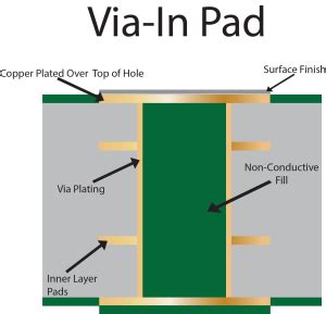
Via Pads: Via pads are used to create electrical connections between different layers of a multi-layer PCB. They consist of drilled holes with conductive plating, allowing signals to pass through the board.
-
Solder Mask Defined (SMD) Pads: SMD pads have a solder mask opening that is smaller than the copper pad size. This helps to control the amount of solder applied to the pad during the soldering process.
-
Non-Solder Mask Defined (NSMD) Pads: NSMD pads have a solder mask opening that is larger than the copper pad size. This allows for more solder to be applied to the pad, which can be beneficial for certain applications.
PCB Pad Design Considerations
When designing PCB pads, several factors need to be taken into account to ensure optimal performance and reliability:
Pad Size and Shape
The size and shape of PCB pads depend on the component package and the specific design requirements. It is essential to follow the manufacturer’s recommended pad dimensions to ensure proper soldering and mechanical stability. Pad sizes that are too small can lead to insufficient solder joint strength, while oversized pads can cause solder bridging and other manufacturing defects.
Pad Spacing
Proper pad spacing is crucial to avoid short circuits and signal interference. The spacing between pads should be sufficient to accommodate the soldering process and prevent solder bridges from forming. The minimum pad spacing is determined by the PCB manufacturing capabilities and the design rules specified by the PCB fabricator.
Thermal Management
PCB pads play a crucial role in thermal management, especially for power-hungry components. Larger pads or thermal pads can be used to dissipate heat more effectively. Thermal vias, which are small holes filled with conductive material, can also be incorporated into the pad design to transfer heat to other layers of the PCB.
Solder Mask and Paste Mask
The solder mask and paste mask openings on PCB pads should be carefully designed to ensure proper solder application and prevent solder bridging. The solder mask opening should be slightly larger than the pad size to allow for tolerances in the manufacturing process. The paste mask opening, on the other hand, should be smaller than the pad size to control the amount of solder paste applied during the assembly process.
Pad Orientation and Placement
The orientation and placement of PCB pads should be considered to optimize signal integrity and minimize interference. Critical signals should be routed away from noisy components, and high-speed signals should have controlled impedance and minimal crosstalk. Proper pad placement can also facilitate easier assembly and rework processes.

PCB Pad Manufacturing Process
The manufacturing process for PCB pads involves several steps:
-
Copper Etching: The copper layer of the PCB is selectively etched away, leaving the desired pad shapes and sizes.
-
Drilling: Holes are drilled through the PCB at the locations of through-hole and via pads.
-
Plating: The drilled holes and pads are plated with a conductive material, typically copper, to ensure electrical connectivity.
-
Solder Mask Application: A solder mask layer is applied over the PCB, leaving openings for the pads and other exposed copper areas.
-
Surface Finish: A surface finish, such as HASL (Hot Air Solder Leveling), ENIG (Electroless Nickel Immersion Gold), or OSP (Organic Solderability Preservative), is applied to the pads to enhance solderability and protect against oxidation.

Best Practices for PCB Pad Design
To ensure optimal performance and manufacturability, consider the following best practices when designing PCB pads:
- Follow the component manufacturer’s recommended pad dimensions and spacing.
- Use appropriate pad sizes and shapes for the specific component package and application.
- Ensure proper solder mask and paste mask openings to control solder application and prevent bridging.
- Consider thermal management requirements and incorporate thermal pads or vias when necessary.
- Optimize pad orientation and placement for signal integrity and ease of assembly.
- Adhere to the PCB fabricator’s design rules and guidelines for pad design and spacing.
- Perform thorough design reviews and simulations to validate pad design and catch potential issues early in the development process.

Common PCB Pad Issues and Troubleshooting
Despite careful design and manufacturing, PCB pads can sometimes encounter issues that affect the performance and reliability of the circuit. Here are some common PCB pad issues and troubleshooting tips:
Solder Bridging
Solder bridging occurs when excess solder forms a conductive bridge between adjacent pads, causing a short circuit. This can be caused by improper solder mask design, excessive solder paste application, or incorrect reflow soldering parameters. To troubleshoot solder bridging:
- Inspect the pads visually or using X-ray imaging to identify the bridged areas.
- Adjust the solder mask opening size or the paste mask aperture to control solder application.
- Optimize the reflow soldering profile to ensure proper solder melting and flow.
- Use a soldering iron or desoldering braid to remove the excess solder and separate the bridged pads.
Pad Lifting
Pad lifting occurs when the pad separates from the PCB surface due to mechanical stress or improper bonding during the manufacturing process. This can lead to intermittent connections or complete signal loss. To troubleshoot pad lifting:
- Inspect the affected pads visually or using microscopy to assess the extent of the lifting.
- Rework the lifted pads by applying additional solder or using conductive epoxy to reattach them to the PCB surface.
- Review the PCB manufacturing process and adhesion parameters to prevent future pad lifting issues.
Insufficient Solder Joint Strength
Insufficient solder joint strength can occur when the pad size is too small or when there is not enough solder applied to the pad. This can result in weak mechanical connections and intermittent electrical contact. To troubleshoot insufficient solder joint strength:
- Verify that the pad dimensions meet the component manufacturer’s recommendations.
- Ensure that the solder paste volume and solder mask opening are adequate for proper solder application.
- Adjust the reflow soldering profile to achieve optimal solder joint formation.
- Consider increasing the pad size or adding additional solder to strengthen the joint.
PCB Pad Design Tools and Software
Various PCB design tools and software are available to assist in creating and optimizing PCB pad layouts. Some popular options include:
-
Altium Designer: A comprehensive PCB design software that offers advanced features for pad design, component placement, and routing.
-
Eagle: A widely used PCB design software that provides a user-friendly interface and extensive libraries for pad and component footprints.
-
KiCad: An open-source PCB design suite that includes tools for schematic capture, PCB layout, and pad design.
-
OrCAD: A powerful PCB design software that offers a range of tools for pad design, simulation, and manufacturing preparation.
These tools provide libraries of pre-defined pad footprints for common component packages, as well as the ability to create custom pad shapes and sizes. They also offer design rule checking (DRC) features to ensure that pad designs meet manufacturing constraints and industry standards.
Frequently Asked Questions (FAQ)
-
What is the difference between SMD and through-hole pads?
SMD (Surface Mount Device) pads are designed for components that are mounted on the surface of the PCB, while through-hole pads are used for components with leads that pass through the board and are soldered on the opposite side. -
How do I determine the appropriate pad size for a component?
The appropriate pad size for a component depends on the specific package and the manufacturer’s recommendations. Refer to the component datasheet or consult the manufacturer’s application notes to determine the recommended pad dimensions. -
What is the purpose of solder mask on PCB pads?
The solder mask is a protective layer applied over the PCB that leaves openings for the pads and other exposed copper areas. It serves to prevent solder bridging, protect against oxidation, and provide electrical insulation between adjacent pads. -
How can I improve the thermal management of PCB pads?
To improve the thermal management of PCB pads, you can increase the pad size to provide more surface area for heat dissipation. Additionally, incorporating thermal vias or using specialized thermal pads can help transfer heat away from the component more effectively. -
What should I do if I encounter solder bridging or pad lifting issues?
If you encounter solder bridging, use a soldering iron or desoldering braid to remove the excess solder and separate the bridged pads. For pad lifting, rework the affected pads by applying additional solder or using conductive epoxy to reattach them to the PCB surface. Review the PCB manufacturing process and parameters to prevent future issues.
Conclusion
PCB pads are critical components in electronic circuit design, providing the necessary connections between components and the copper traces on the board. Understanding the types of pads, design considerations, and best practices is essential for creating reliable and high-performance PCBs.
By following the guidelines outlined in this article, such as selecting appropriate pad sizes and shapes, ensuring proper spacing, and considering thermal management requirements, designers can optimize their PCB pad layouts for manufacturability and functionality.
Additionally, utilizing PCB design tools and software can streamline the pad design process, providing access to libraries of pre-defined footprints and design rule checking features to ensure compliance with industry standards.
As technology advances and electronic devices become more complex, the importance of well-designed PCB pads cannot be overstated. By staying up-to-date with the latest design techniques and best practices, engineers and designers can create PCBs that meet the demanding requirements of modern electronic applications.


Leave a Reply