Introduction to PCB Fabrication
Printed Circuit Board (PCB) fabrication is a complex process that involves multiple steps to create a functional board. One of the crucial stages in PCB fabrication is the lay-up and bonding of multiple layers to form a multi-layer PCB. This process requires precision, accuracy, and strict adherence to industry standards to ensure the final product meets the desired specifications.
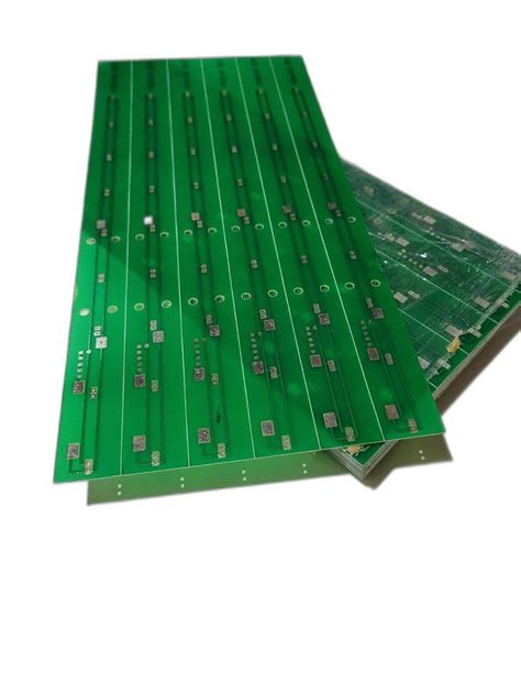
Understanding Multi-layer PCBs
Multi-layer PCBs consist of multiple layers of conductive copper and insulating material, typically FR-4, bonded together to form a single board. The number of layers can vary depending on the complexity of the design and the application requirements. Some common multi-layer PCB configurations include:
| Layers | Description |
|---|---|
| 4 | Double-sided board with two internal layers |
| 6 | Double-sided board with four internal layers |
| 8 | Double-sided board with six internal layers |
| 10+ | Complex boards with eight or more internal layers |
The main advantage of multi-layer PCBs is the ability to accommodate more components and complex circuits in a smaller footprint compared to single or double-layer boards.

Lay-up Process
The lay-up process involves stacking the individual layers of the PCB in the correct order and orientation before bonding them together. The steps involved in the lay-up process are as follows:
1. Layer Preparation
Each layer of the PCB is prepared by applying a photoresist coating to the copper surface. The photoresist is then exposed to UV light through a photomask, which contains the circuit pattern for that specific layer. The unexposed photoresist is then removed, leaving behind the desired copper pattern.
2. Layer Stacking
The prepared layers are then stacked in the correct order, with the outer layers (top and bottom) placed on the outside and the inner layers sandwiched between them. The layers are aligned using registration holes or Fiducial Marks to ensure proper positioning.
3. Bonding Sheet Placement
A bonding sheet, typically made of prepreg (pre-impregnated) material, is placed between each layer. The prepreg contains a resin that flows and fills the gaps between the layers during the bonding process, creating a strong adhesive bond.
4. Lay-up Registration
The stacked layers and bonding sheets are then placed in a lay-up press, which applies pressure and heat to the stack. The registration holes or fiducial marks are used to ensure the layers remain aligned during the pressing process.

Bonding Process
The bonding process involves applying heat and pressure to the stacked layers to cure the prepreg resin and create a solid, unified board. The steps involved in the bonding process are as follows:
1. Vacuum Lamination
The stacked layers are placed in a vacuum lamination press, which removes any air trapped between the layers. This ensures a tight, void-free bond between the layers.
2. Heating and Pressing
The lamination press then applies heat and pressure to the stack for a specific duration, typically ranging from 1 to 2 hours, depending on the thickness of the board and the type of prepreg used. The heat causes the prepreg resin to flow and cure, bonding the layers together.
| Parameter | Value Range |
|---|---|
| Temperature | 180°C – 200°C |
| Pressure | 200 – 400 psi |
| Duration | 1 – 2 hours |
3. Cooling and Removal
After the bonding cycle is complete, the press is cooled down gradually to room temperature. The bonded board is then removed from the press and inspected for any defects or misalignment.

Post-Bonding Processes
After the bonding process, the multi-layer PCB undergoes several post-bonding processes to create the final product. These processes include:
1. Drilling
Holes are drilled through the board to accommodate component leads and vias that connect the different layers. The drilling process is performed using high-speed CNC machines with carbide drill bits.
2. Plating
The drilled holes are then plated with copper to create electrical connections between the layers. This is typically done using electroless copper plating followed by electroplating to achieve the desired thickness.
3. Outer Layer Imaging
The outer layers of the board are then imaged with the final circuit pattern using a process similar to the inner layer preparation. The photoresist is applied, exposed, and developed to create the desired copper pattern.
4. Etching and Finishing
The exposed copper is then etched away, leaving behind the final circuit pattern. The board is then finished with a protective solder mask and surface finish, such as HASL (Hot Air Solder Leveling) or ENIG (Electroless Nickel Immersion Gold).
Quality Control and Inspection
Throughout the PCB fabrication process, strict quality control measures are implemented to ensure the final product meets the required specifications. Some of the key quality control steps include:
1. Visual Inspection
Each layer of the PCB is visually inspected for defects, such as shorts, opens, or misalignment, before proceeding to the next step.
2. Electrical Testing
The finished board undergoes electrical testing to verify continuity, insulation resistance, and other electrical parameters. This is typically done using automated testing equipment, such as Flying probe testers or bed-of-nails fixtures.
3. Microsectioning
In some cases, a microsection analysis may be performed to verify the internal structure of the board, such as the layer alignment, bonding quality, and plating thickness. This involves cross-sectioning the board and examining it under a microscope.
Conclusion
PCB multi-layer fabrication is a complex process that requires precision, accuracy, and strict adherence to industry standards. The lay-up and bonding processes are critical steps in creating a functional and reliable multi-layer PCB. By understanding the various steps involved and implementing proper quality control measures, PCB Manufacturers can produce high-quality boards that meet the demanding requirements of modern electronic devices.
Frequently Asked Questions (FAQ)
1. What is the purpose of using prepreg in the bonding process?
Prepreg, or pre-impregnated material, is used as a bonding sheet between the layers of a multi-layer PCB. It contains a partially cured resin that flows and fills the gaps between the layers during the bonding process, creating a strong adhesive bond. The prepreg also acts as an insulating layer between the conductive copper layers.
2. How does the number of layers affect the complexity of the PCB fabrication process?
As the number of layers in a PCB increases, the fabrication process becomes more complex. With more layers, there are more opportunities for defects, such as misalignment or delamination, to occur. The lay-up and bonding processes also take longer, as there are more layers to stack and bond together. Additionally, the drilling and plating processes become more challenging, as the holes must be precisely aligned through all layers.
3. What are the advantages of using a vacuum lamination press in the bonding process?
A vacuum lamination press is used to remove any air trapped between the layers of the PCB before applying heat and pressure. This ensures a tight, void-free bond between the layers, reducing the risk of delamination and improving the overall reliability of the board. The vacuum also helps to evenly distribute the pressure across the surface of the board, resulting in a more consistent bond.
4. What is the purpose of microsectioning in quality control?
Microsectioning is a quality control technique that involves cross-sectioning a sample of the PCB and examining it under a microscope. This allows the manufacturer to verify the internal structure of the board, such as the layer alignment, bonding quality, and plating thickness. Microsectioning is particularly useful for detecting defects that may not be visible through external inspection, such as voids or delamination between layers.
5. How does the choice of surface finish affect the performance of the PCB?
The choice of surface finish can have a significant impact on the performance and reliability of the PCB. Different surface finishes have different properties, such as solderability, durability, and shelf life. For example, HASL (Hot Air Solder Leveling) is a common surface finish that provides good solderability but may have a limited shelf life due to oxidation. On the other hand, ENIG (Electroless Nickel Immersion Gold) provides excellent solderability and shelf life but may be more expensive than other options. The choice of surface finish depends on the specific application requirements and the manufacturing budget.


Leave a Reply