Introduction
Designing a printed circuit board (PCB) layout is a complex process that requires careful consideration of various factors to ensure optimal performance, reliability, and manufacturability. In this article, we will explore six crucial aspects that you should keep in mind when designing your PCB layout. By understanding and implementing these considerations, you can create a robust and efficient PCB that meets your project’s requirements.
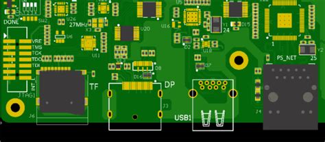
1. Component Placement
a. Grouping Components
When placing components on your PCB, it’s essential to group them based on their functionality and interconnectivity. This approach helps minimize the length of traces, reduces signal interference, and improves the overall performance of your circuit. Consider dividing your PCB into logical sections, such as power supply, analog, digital, and high-frequency regions, to facilitate proper component placement.
b. Thermal Management
Pay attention to the thermal characteristics of your components, especially power-hungry devices like voltage regulators, power transistors, and high-speed processors. Place these components in areas with adequate cooling, such as near the edge of the board or in proximity to heat sinks. Ensure sufficient spacing between heat-generating components to prevent thermal interference and overheating.
c. Mechanical Constraints
Consider the mechanical constraints of your PCB, such as the enclosure size, mounting holes, and connector locations. Place components in a way that allows for easy assembly, reduces strain on the board, and accommodates any necessary mechanical support structures. Keep in mind the accessibility of components for debugging, testing, and potential repairs.

2. Signal Integrity
a. Trace Routing
Proper trace routing is crucial for maintaining signal integrity and minimizing electromagnetic interference (EMI). Keep high-speed signals as short as possible and route them away from sensitive analog circuits. Use appropriate trace widths based on the current carrying capacity and impedance requirements. Avoid sharp angles and use smooth curves or 45-degree angles when changing trace directions to reduce reflections and signal distortion.
b. Impedance Matching
For high-speed signals, it’s crucial to match the impedance of the traces to the source and load impedances to minimize reflections and ensure proper signal propagation. Use controlled impedance techniques, such as micro-strip or strip-line routing, and adjust the trace width and spacing to achieve the desired impedance. Consider the dielectric constant and thickness of the PCB substrate when calculating impedance.
c. Crosstalk Mitigation
Crosstalk occurs when signals from one trace interfere with adjacent traces, leading to signal integrity issues. To mitigate crosstalk, ensure adequate spacing between parallel traces, especially for high-speed signals. Use ground planes or guard traces to provide shielding and isolation between sensitive signals. In multi-layer PCBs, route critical signals on inner layers surrounded by ground planes to minimize crosstalk.

3. Power Distribution Network (PDN)
a. Power Plane
Dedicate one or more layers of your PCB to power planes, which provide a low-impedance path for distributing power to components. Use separate power planes for different voltage levels to minimize noise coupling. Ensure that the power planes have sufficient copper thickness to handle the required current and minimize voltage drop.
b. Decoupling Capacitors
Place decoupling capacitors close to the power pins of digital ICs to provide a stable and clean power supply. Use a combination of bulk, ceramic, and small-value capacitors to cover different frequency ranges and suppress power supply noise. Minimize the loop area between the capacitor and the IC power pin to reduce parasitic inductance.
c. Power Integrity Analysis
Perform power integrity analysis to ensure that your PDN can deliver the required current to all components without excessive voltage drop or noise. Use simulation tools to analyze the impedance profile of your PDN and identify potential resonance or instability issues. Optimize the placement and values of decoupling capacitors based on the analysis results.

4. Grounding
a. Ground Plane
Implement a solid ground plane on one or more layers of your PCB to provide a low-impedance return path for signals and minimize ground loops. Connect all ground pins of components to the ground plane using short traces or vias. Avoid splitting the ground plane unnecessarily, as it can create ground loops and degrade signal integrity.
b. Grounding Techniques
Use appropriate grounding techniques based on the frequency and sensitivity of your signals. For low-frequency analog circuits, use a single-point ground connection to minimize ground loops. For high-frequency digital circuits, use a multi-point ground connection to provide a low-impedance return path. Separate analog and digital ground planes, and connect them at a single point to prevent noise coupling.
c. ESD Protection
Incorporate electrostatic discharge (ESD) protection measures in your PCB design to prevent damage to sensitive components. Place ESD protection devices, such as transient voltage suppressors (TVS) or ESD diodes, near the external connectors or interfaces. Route ESD-sensitive signals through protected paths and use guard rings or shielding to minimize ESD coupling.
5. Manufacturing Considerations
a. Design for Manufacturing (DFM)
Follow the design for manufacturing (DFM) guidelines provided by your PCB Fabrication and assembly partners. Adhere to the minimum trace width, spacing, and hole size requirements to ensure manufacturability. Use standard component footprints and avoid uncommon or custom packages to simplify the assembly process. Include fiducial markers and test points to facilitate automated assembly and testing.
b. Panelization
If your PCB design is small, consider panelizing multiple copies of the board on a single panel to reduce manufacturing costs and improve efficiency. Include v-scoring or tab routing features to allow easy separation of individual boards after assembly. Provide sufficient spacing between boards to accommodate the panelization process and avoid potential damage during depaneling.
c. Solder Mask and Silkscreen
Use solder mask to protect the copper traces from oxidation and prevent accidental short circuits during soldering. Define appropriate solder mask openings for component pads and vias. Include clear and legible silkscreen markings to indicate component designators, polarity, and other relevant information. Ensure that the silkscreen does not overlap with solder mask openings or component pads.
6. Testing and Debugging
a. Test Points
Include test points in your PCB layout to facilitate testing and debugging. Place test points at critical nodes or signals that require probing or measurement. Use appropriate test point sizes and spacing to accommodate test probes and avoid interference with nearby components. Consider using dedicated test headers or connectors for complex testing scenarios.
b. Boundary Scan
If your design includes complex digital circuits or high pin-count ICs, consider implementing boundary scan (JTAG) testing capabilities. Boundary scan allows for testing and debugging of individual components and interconnects without the need for physical access. Include JTAG test points and connectors in your PCB layout and ensure proper routing of the JTAG signals.
c. Design for Testability (DFT)
Incorporate design for testability (DFT) principles in your PCB layout to simplify testing and debugging processes. Use test pads or vias to provide access to critical signals for probing. Consider adding built-in self-test (BIST) circuits or logic analyzers to enable in-system testing and diagnostics. Design your PCB with modularity in mind, allowing for easy isolation and testing of individual subsystems.
Frequently Asked Questions (FAQ)
1. What is the importance of component placement in PCB layout?
Component placement is crucial in PCB layout as it directly impacts the performance, reliability, and manufacturability of the circuit. Proper component placement helps minimize trace lengths, reduces signal interference, improves thermal management, and facilitates efficient assembly and testing processes.
2. How can I ensure signal integrity in my PCB layout?
To ensure signal integrity in your PCB layout, consider the following practices:
– Route high-speed signals as short as possible and away from sensitive analog circuits.
– Use appropriate trace widths and impedance matching techniques.
– Minimize crosstalk by providing adequate spacing between parallel traces and using ground planes or guard traces for shielding.
– Perform signal integrity simulations to analyze and optimize the behavior of critical signals.
3. What is the purpose of a power plane in a PCB?
A power plane in a PCB serves as a low-impedance path for distributing power to components. It provides a stable and uniform power supply, minimizes voltage drop, and reduces power supply noise. Power planes are typically dedicated to specific voltage levels and are separated from other signal layers to minimize noise coupling.
4. How do I implement effective grounding in my PCB layout?
Effective grounding in PCB layout involves the following practices:
– Use a solid ground plane to provide a low-impedance return path for signals and minimize ground loops.
– Connect all ground pins of components to the ground plane using short traces or vias.
– Separate analog and digital ground planes and connect them at a single point to prevent noise coupling.
– Use appropriate grounding techniques based on the frequency and sensitivity of signals, such as single-point or multi-point grounding.
5. What are the key considerations for manufacturing-friendly PCB layout?
To create a manufacturing-friendly PCB layout, consider the following:
– Follow the design for manufacturing (DFM) guidelines provided by your PCB fabrication and assembly partners.
– Adhere to the minimum trace width, spacing, and hole size requirements.
– Use standard component footprints and avoid uncommon or custom packages.
– Include fiducial markers, test points, and clear silkscreen markings to facilitate automated assembly and testing.
– Consider panelization for small PCBs to reduce manufacturing costs and improve efficiency.
Conclusion
Designing a PCB layout requires careful consideration of various factors to ensure optimal performance, reliability, and manufacturability. By focusing on component placement, signal integrity, power distribution, grounding, manufacturing considerations, and testing, you can create a robust and efficient PCB that meets your project’s requirements. Remember to follow best practices, adhere to design guidelines, and collaborate with your manufacturing partners to achieve the best results. With a well-designed PCB layout, you can bring your electronic projects to life with confidence and success.
| Consideration | Key Points |
|---|---|
| Component Placement | – Group components based on functionality and interconnectivity – Consider thermal management and mechanical constraints – Ensure accessibility for debugging and testing |
| Signal Integrity | – Minimize trace lengths and route high-speed signals away from sensitive circuits – Use appropriate trace widths and impedance matching techniques – Mitigate crosstalk through spacing, ground planes, and guard traces |
| Power Distribution Network | – Dedicate layers for power planes to provide low-impedance power distribution – Place decoupling capacitors close to IC power pins – Perform power integrity analysis to optimize PDN performance |
| Grounding | – Implement a solid ground plane for low-impedance return path – Use appropriate grounding techniques based on signal frequency and sensitivity – Separate analog and digital ground planes and connect them at a single point |
| Manufacturing Considerations | – Follow design for manufacturing (DFM) guidelines – Adhere to minimum trace width, spacing, and hole size requirements – Use standard component footprints and consider panelization for small PCBs |
| Testing and Debugging | – Include test points at critical nodes for probing and measurement – Implement boundary scan (JTAG) testing for complex digital circuits – Incorporate design for testability (DFT) principles to simplify testing and debugging |
By considering these six important aspects and implementing the best practices associated with each, you can create a well-designed PCB layout that meets your project’s requirements and ensures optimal performance, reliability, and manufacturability.


Leave a Reply