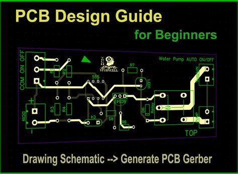
Introduction to PCB Drafting
Printed Circuit Board (PCB) drafting is a critical process in the design and manufacture of electronic devices. It involves creating detailed drawings that provide a visual representation of the PCB layout, components, and connections. Adhering to established drafting standards is essential to ensure the accuracy, clarity, and consistency of PCB drawings.
In this article, we will explore five key drafting standards that should be followed when creating PCB drawings. These standards cover various aspects, including schematic symbols, layer stackup, component placement, routing, and documentation. By understanding and applying these standards, PCB designers can create high-quality drawings that facilitate efficient manufacturing and minimize the risk of errors.
1. Schematic Symbol Standards
1.1 Symbol Libraries
- Use standardized symbol libraries for consistency
- Ensure symbols are clear, legible, and easily recognizable
- Follow industry-standard symbol conventions (e.g., IEEE, IEC)
1.2 Symbol Sizing and Proportions
- Maintain consistent symbol sizes throughout the schematic
- Use appropriate proportions for symbol elements (e.g., pins, labels)
- Avoid overcrowding or overlapping symbols
1.3 Pin Labeling and Numbering
- Label pins with clear and concise names
- Use sequential numbering for multi-pin components
- Align pin labels and numbers for readability

2. Layer Stackup Standards
2.1 Layer Arrangement
- Follow a logical layer stackup order (e.g., signal, ground, power)
- Use dedicated layers for specific purposes (e.g., routing, shielding)
- Maintain consistent layer spacing and thickness
2.2 Layer Naming Conventions
- Use descriptive and standardized layer names
- Differentiate between signal, plane, and mechanical layers
- Include layer numbers or identifiers for easy reference
2.3 Copper Weight and Thickness
- Specify the appropriate copper weight for each layer
- Consider the current carrying capacity and signal integrity requirements
- Ensure consistent copper thickness across the PCB

3. Component Placement Standards
3.1 Component Orientation
- Orient components for optimal routing and assembly
- Align components with respect to the board edges and reference designators
- Consider component height and clearance requirements
3.2 Component Spacing
- Maintain adequate spacing between components for manufacturing and assembly
- Follow recommended minimum spacing guidelines based on component package types
- Consider thermal dissipation and electrical isolation requirements
3.3 Reference Designators
- Assign unique and sequential reference designators to each component
- Use a consistent format for reference designators (e.g., R1, C2, U3)
- Place reference designators near the component for easy identification

4. Routing Standards
4.1 Trace Width and Spacing
- Select appropriate trace widths based on current carrying capacity and signal integrity
- Maintain consistent trace spacing to minimize crosstalk and interference
- Follow recommended trace width and spacing guidelines for the chosen PCB technology
4.2 Via Placement and Sizing
- Place vias strategically to minimize signal reflections and EMI
- Use appropriate via sizes based on the current carrying capacity and layer transitions
- Avoid placing vias too close to component pads or other vias
4.3 Routing Techniques
- Use clean and efficient routing paths to minimize signal length and impedance discontinuities
- Avoid sharp angles and unnecessary jogs in traces
- Consider the use of routing constraints and design rules for automated routing
5. Documentation Standards
5.1 Schematic Annotations
- Provide clear and concise annotations on the schematic
- Include component values, tolerances, and ratings
- Specify any special instructions or requirements for manufacturing or assembly
5.2 Bill of Materials (BOM)
- Generate a complete and accurate BOM
- Include component part numbers, quantities, and descriptions
- Specify any alternate or substitute components if applicable
5.3 Assembly Drawings
- Create detailed assembly drawings that show component placement and orientation
- Include dimensions, tolerances, and any special assembly instructions
- Provide clear and legible labels for reference designators and component identifiers
Frequently Asked Questions (FAQ)
1. What are the benefits of following PCB drafting standards?
Following PCB drafting standards offers several benefits:
– Consistency and clarity in PCB drawings across different projects and designers
– Improved communication between design, manufacturing, and assembly teams
– Reduced risk of errors and misinterpretations
– Faster design review and approval processes
– Enhanced manufacturability and assembly efficiency
2. Are there any industry-specific PCB drafting standards?
Yes, there are industry-specific PCB drafting standards that cater to the unique requirements of different sectors, such as:
– IPC standards for the electronics industry
– JEDEC standards for semiconductor and microelectronics
– Mil-spec standards for military and aerospace applications
– Automotive standards for vehicle electronics
3. How can I ensure compliance with PCB drafting standards?
To ensure compliance with PCB drafting standards, you can:
– Familiarize yourself with the relevant standards and guidelines
– Use standardized libraries and templates for consistency
– Implement design rule checks (DRC) in your PCB design software
– Conduct regular design reviews and audits
– Seek feedback from manufacturing and assembly partners
4. What are the consequences of not following PCB drafting standards?
Not following PCB drafting standards can lead to various issues, such as:
– Misinterpretation of design intent
– Errors in manufacturing and assembly
– Delays in project timelines
– Increased costs due to rework and redesign
– Compromised product quality and reliability
5. How often should PCB drafting standards be updated?
PCB drafting standards should be reviewed and updated periodically to keep pace with advancements in technology, manufacturing processes, and industry best practices. The frequency of updates may vary depending on the specific standards and the industry sector. It is essential to stay informed about the latest revisions and updates to ensure compliance and maintain best practices in PCB design and drafting.
Conclusion
Adhering to PCB drafting standards is crucial for creating accurate, clear, and consistent PCB drawings. By following the five key standards discussed in this article – schematic symbols, layer stackup, component placement, routing, and documentation – PCB designers can streamline the design process, improve communication with manufacturing and assembly teams, and minimize the risk of errors.
Investing time and effort in understanding and applying these drafting standards will ultimately lead to higher-quality PCB designs, faster time-to-market, and reduced costs associated with rework and redesign. As PCB technology continues to evolve, it is essential for designers to stay updated with the latest standards and best practices to ensure the success of their projects.
| Standard Category | Key Aspects |
|---|---|
| Schematic Symbols | – Symbol libraries – Symbol sizing and proportions – Pin labeling and numbering |
| Layer Stackup | – Layer arrangement – Layer naming conventions – Copper weight and thickness |
| Component Placement | – Component orientation – Component spacing – Reference designators |
| Routing | – Trace width and spacing – Via placement and sizing – Routing techniques |
| Documentation | – Schematic annotations – Bill of Materials (BOM) – Assembly drawings |
Table 1: Summary of PCB Drafting Standards
By adhering to these PCB drafting standards and continuously refining your design practices, you can create high-quality PCB drawings that facilitate efficient manufacturing, assembly, and ultimately, the success of your electronic products.


Leave a Reply