What is DFM in PCB Design?
DFM (Design for Manufacturability) is the process of proactively designing products to optimize all manufacturing functions – fabrication, assembly, test, procurement, shipping, delivery, service, and repair. The goal is to achieve the lowest possible total cost while maintaining the required quality and reliability.
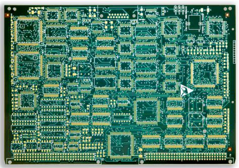
In the context of PCB design, DFM means incorporating manufacturing considerations upfront during the design stage. This involves following certain guidelines related to component selection and placement, routing, power distribution, thermal management, testing, and documentation – all with the aim of making the board easier and more cost-effective to manufacture with minimal defects.
Some key benefits of applying DFM principles to PCB design include:
- Lower production costs
- Improved yield rates
- Faster time-to-market
- Enhanced product quality and reliability
- Easier assembly and rework
- Smoother transition from prototype to mass production
DFM Guidelines for PCB Component Selection and Placement
One of the most important aspects of PCB design for manufacturability is selecting the right components and positioning them optimally on the board. Here are some DFM guidelines to follow:
Use Standard Components When Possible
Using standard, widely available components from established suppliers makes the BOM (Bill of Materials) more predictable from a cost, lead time and quality standpoint. Custom or obsolete parts increase supply chain risk.
Pay Attention to Component Footprint and Package
Make sure to use component footprints that match the manufacturing capabilities in terms of pitch, pad size, spacing, etc. Fine-pitch parts (<0.5mm) require more precise and expensive assembly equipment. SMT is generally preferable to through-hole in terms of manufacturability. If using through-hole, pay attention to lead forming and hole size.
Adhere to Minimum Spacing Requirements
Maintain proper spacing between components based on the assembly process and equipment to avoid manufacturing issues. Typical minimum values are:
| Manufacturing Process | Minimum Component Spacing |
|---|---|
| Through-hole hand assembly | 0.2″ (5.08 mm) |
| Through-hole wave solder | 0.3″ (7.62 mm) |
| SMT reflow soldering | 0.04″ (1.0 mm) |
Optimize Component orientation
Orient components in the same direction as much as possible for more efficient Solder Paste application and visual inspection. Avoid parts that must be inserted at odd angles.
Component Placement for Ease of Assembly
Group similar components together to speed up the assembly process. Place parts strategically for an efficient assembly flow – for example, heaviest parts towards the center, smallest parts last, connectors near board edges, etc.
Avoid placing parts too close to board edges to prevent overhang during wave soldering. Provide proper clearance around sensitive components like crystals and RF shields.

DFM Considerations for PCB Routing and Copper
Proper routing and copper design is critical for PCB manufacturability, signal integrity, power integrity and EMC. Keep the following guidelines in mind:
Use Proper Trace Width and Spacing
- Traces that are too thin (<3 mil) are prone to peeling and damage. Go wider when possible.
- Maintain proper clearance between traces, pads and vias to avoid short circuits. Typical minimums:
| Copper Feature | Minimum Spacing (Cheap) | Minimum Spacing (Standard) | Minimum Spacing (Advanced) |
|---|---|---|---|
| Trace to trace | 8 mil (0.2mm) | 6 mil (0.15 mm) | 4 mil (0.1mm) |
| Trace to pad/via | 10 mil (0.25 mm) | 8 mil (0.2 mm) | 6 mil (0.15 mm) |
| SMD pad to pad | 10 mil (0.25 mm) | 8 mil (0.2 mm) | 6 mil (0.15 mm) |
Route for Efficient Panelization
Orient the board outline such that multiple copies can be efficiently panelized on a standard panel size with minimal waste. Avoid irregular board shapes when possible. Use score lines or V-grooves for depaneling.
Optimize Via Usage
Vias add to manufacturing cost and impact signal integrity when overused. Minimize layer transitions and through-hole vias. Use proper via size for the hole/annular ring. Avoid vias under BGA pads.
Define Proper Pad Sizes
The pad size must be appropriate for the component lead/pin and soldering process. Typical recommendations:
| Pad Type | Minimum Size | Preferred Size |
|---|---|---|
| SOIC, SOT SMD | 16 x 32 mil | 24 x 48 mil |
| TQFP, QFP SMD | 12 x 18 mil | 16 x 24 mil |
| Chip SMD | 20 x 30 mil | 28 x 50 mil |
| Through-hole | 20 mil larger than hole | 30-40 mil larger than hole |
Manage Copper Balance and Density
- Ensure even Copper Distribution across layers to prevent warpage during manufacturing.
- Avoid abrupt copper density changes which may cause acid traps and etching issues.
- Add copper thieving/fill if needed to equalize copper coverage.

Planning for PCB Test and Inspection
Making a PCB easier to test and inspect is a key part of Design for Manufacturability. Consider the following:
Add Fiducials for Machine Vision Alignment
Include fiducial marks on the outer layers for automated optical inspection (AOI) systems and pick-and-place machines to register the board position. Use a non-solder mask defined copper shape, typically a circle or cross, near the corners of the board. Optimal fiducial size is 1mm.
Provide Test Points and Probe Access
Add test points on key signals, power rails and ground for in-circuit testing (ICT). Make sure the probe targets are accessible and not obstructed by taller components. Use SMD test points of size 0.04″ minimum.
Allow Space for Tooling/Identification Marks
Provide space on the board, typically near an edge, for manufacturing-related marks such as part number, UL certification, ESD warning, bar code, date code, etc. This aids in tracking and traceability.

Thermal Management and Power Distribution
Proper thermal management and power integrity are essential for a manufacturable, reliable PCB. Keep these points in mind:
Manage Power Dissipation
Identify hot components and provide adequate heatsinking using copper pour, thermal vias, heatsinks, etc. Avoid placing hot parts near thermally sensitive components.
Optimize Power Distribution
Use appropriate trace width for power nets based on current. Provide solid ground and power planes when possible. Decouple ICs properly with local capacitors. Avoid daisy-chaining power.
Documentation for Manufacturability
Clear, comprehensive documentation is a must for ensuring the PCB design intent is properly communicated to the manufacturer. This includes:
Schematic with Key Information
- Reference designators
- Component values
- Pin names and numbers
- Power rail specifications
- Special instructions
Layout Files in Industry Standard Format
- Gerber files (RS-274X)
- NC drill files (Excellon)
- Pick-and-place file (CSV or ASCII)
Detailed Bill of Materials (BOM)
- Manufacturer part numbers
- Reference designators
- Quantities
- Alternates/substitutes if applicable
Fabrication Drawing with Specs
- Board outline dimensions
- Layer stackup
- Drill chart and hole sizes
- Material specifications
- Surface finish
- Impedance requirements
- Special instructions
Assembly Drawing
- Component placement
- Reference designator pointing
- Assembly notes
- Variants/options
Frequently Asked Questions (FAQ) About PCB Design for Manufacturability
Q1. What is the most important factor in PCB design for manufacturability?
A1. While all DFM guidelines are important, component selection and placement arguably have the biggest impact on manufacturability. Using standard parts with proper footprints and spacing is critical for cost-effective, high-yield assembly.
Q2. Is it always better to use SMT Components over through-hole for DFM?
A2. In general, yes – SMT allows for automated assembly and higher component density compared to through-hole. However, through-hole still has its place for certain connectors, structural parts, or high-power components. The key is to minimize mixing SMT and through-hole to avoid double-sided reflow or wave soldering.
Q3. What’s the best way to ensure the PCB fabricator and assembler can properly manufacture my design?
A3. Provide complete, accurate documentation including the schematic, BOM, layout files, fabrication drawing and assembly drawing. Call out all critical specifications. Follow up with questions to resolve any ambiguities.
Q4. How do I manage the tradeoffs between PCB manufacturability and other design requirements like performance or size?
A4. It’s a balancing act. Involve the manufacturer early in the design process to understand their capabilities and tolerances. Make smart compromises. For example, use smaller components and tighter spacing only in critical areas rather than the entire board. Consider panelization for very small boards.
Q5. What’s the most common DFM mistake you see in PCB designs?
A5. One of the most common issues is improper solder mask clearance around pads, which can cause open circuits or solder shorts. Another is using inadequate trace width for power nets, leading to voltage drop or overheating. Thankfully, most modern PCB design tools have DFM rule checks to catch such errors.
In summary, incorporating DFM principles throughout the PCB design process – from component selection and placement to routing, documentation and testing – is essential for ensuring high-quality, cost-effective, and timely manufacturing. By paying attention to the guidelines covered in this article, PCB designers can optimize their designs for manufacturability and reap the benefits of a smoother transition from prototype to mass production.


Leave a Reply