Introduction to PCB Soldering
PCB (Printed Circuit Board) soldering is a crucial process in the manufacturing of electronic devices. It involves the attachment of various components, including chip packages, to the surface of a PCB using solder, a metal alloy that melts at a relatively low temperature. Proper soldering ensures reliable electrical connections and mechanical stability of the components on the PCB.
Types of PCB Soldering
There are two main types of PCB soldering:
- Through-hole soldering
- Surface mount soldering (SMT)
Through-hole soldering involves inserting component leads through holes drilled in the PCB and soldering them on the opposite side. This method is less common in modern electronics due to the increased density of components and the need for smaller form factors.
Surface mount soldering, on the other hand, involves placing components directly on the surface of the PCB and soldering them in place. This method allows for higher component density and smaller PCB sizes, making it the preferred choice for most modern electronic devices.
PCB Chip Package Types
Before discussing the soldering process, it is essential to understand the various types of chip packages used in PCB assembly. Some common chip package types include:
- Dual In-line Package (DIP)
- Small Outline Integrated Circuit (SOIC)
- Quad Flat Package (QFP)
- Ball Grid Array (BGA)
- Chip Scale Package (CSP)
Each package type has its unique characteristics, such as lead pitch, size, and thermal properties, which affect the soldering process and requirements.

PCB Soldering Process Flow
The PCB soldering process typically follows these steps:
- PCB Preparation
- Solder Paste Application
- Component Placement
- Reflow Soldering
- Inspection and Rework
1. PCB Preparation
Before soldering, the PCB must be cleaned and prepared to ensure optimal soldering results. This step involves:
- Cleaning the PCB surface to remove any contaminants or oxidation
- Applying a solder mask to protect the PCB surface and prevent solder bridges
- Applying a solder paste stencil to deposit solder paste on the PCB pads
2. Solder Paste Application
Solder paste, a mixture of tiny solder particles and flux, is applied to the PCB pads using a stencil or screen printing process. The stencil ensures that the correct amount of solder paste is deposited on each pad, while the flux helps to clean the surfaces and promote proper solder wetting during the reflow process.
3. Component Placement
After applying the solder paste, the chip packages and other components are placed on the PCB using a pick-and-place machine or by hand. Accurate component placement is crucial to ensure proper alignment with the PCB pads and prevent component shifting during the reflow process.
4. Reflow Soldering
The PCB with the placed components is then subjected to a reflow soldering process, which involves heating the entire assembly in a controlled manner to melt the solder paste and form a permanent connection between the components and the PCB pads. The reflow soldering process typically follows a temperature profile that includes:
- Preheat: Gradually raising the temperature to activate the flux and remove any moisture
- Soak: Maintaining a stable temperature to ensure even heat distribution
- Reflow: Raising the temperature above the solder’s melting point to allow the solder to flow and form a connection
- Cooling: Gradually lowering the temperature to solidify the solder joints
5. Inspection and Rework
After the reflow soldering process, the PCB undergoes a visual inspection to identify any soldering defects, such as:
- Solder bridges: Unintended connections between adjacent pads
- Cold joints: Weak or incomplete solder connections
- Tombstoning: Components standing on one end due to uneven heating or pad design
If any defects are found, a rework process is performed to correct the issues, which may involve manual soldering, desoldering, or component replacement.

Soldering Methods for Different Chip Packages
Different chip packages require specific soldering methods and considerations to ensure optimal results. Some common soldering methods for various chip packages include:
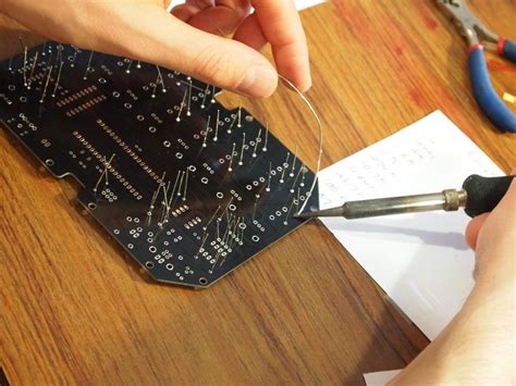
DIP and SOIC Packages
DIP and SOIC packages have leads that extend from the sides of the package and are relatively easy to solder. The soldering process typically involves:
- Applying a small amount of solder to the PCB pad using a soldering iron
- Placing the component lead on the solder and heating it with the soldering iron to form a connection
- Inspecting the solder joint for proper wetting and shape
QFP Packages
QFP packages have leads on all four sides of the package, making them more challenging to solder than DIP or SOIC packages. The soldering process for QFP packages often involves:
- Applying solder paste to the PCB pads using a stencil
- Placing the QFP package on the PCB using a pick-and-place machine or by hand
- Reflowing the solder using a controlled temperature profile
- Inspecting the solder joints for defects and performing rework if necessary
BGA Packages
BGA packages have an array of solder balls on the bottom of the package, which are used to form connections with the PCB pads. Soldering BGA packages requires precise alignment and temperature control, and typically involves:
- Applying solder paste to the PCB pads using a stencil
- Placing the BGA package on the PCB using a pick-and-place machine with high accuracy
- Reflowing the solder using a controlled temperature profile optimized for the specific BGA package
- Inspecting the solder joints using X-ray imaging to identify any defects or voids
- Performing rework, if necessary, using specialized BGA Rework stations
| Package Type | Soldering Method |
|---|---|
| DIP, SOIC | Manual soldering with soldering iron |
| QFP | Solder paste application, reflow soldering |
| BGA | Solder paste application, precise placement, reflow soldering, X-ray inspection |

Factors Affecting PCB Soldering Quality
Several factors can impact the quality of PCB soldering, including:
- Solder paste quality and storage conditions
- PCB and component cleanliness
- Solder paste application accuracy and consistency
- Component placement accuracy
- Reflow temperature profile and control
- PCB design and pad geometry
- Operator skill and experience
To ensure high-quality soldering results, it is essential to control these factors through proper process design, equipment maintenance, and operator training.
Frequently Asked Questions (FAQ)
1. What is the difference between through-hole and surface mount soldering?
Through-hole soldering involves inserting component leads through holes in the PCB and soldering them on the opposite side, while surface mount soldering involves placing components directly on the surface of the PCB and soldering them in place.
2. What is the purpose of applying flux during the soldering process?
Flux helps to clean the surfaces of the PCB pads and component leads, removing oxidation and promoting proper solder wetting during the soldering process. This ensures a strong and reliable solder connection.
3. What is the main advantage of using a reflow soldering process?
Reflow soldering allows for the simultaneous soldering of multiple components on a PCB, making it a highly efficient and cost-effective method for high-volume production. It also ensures consistent and reliable solder joints by using a controlled temperature profile.
4. How can soldering defects be identified and corrected?
Soldering defects can be identified through visual inspection, automated optical inspection (AOI), or X-ray imaging, depending on the component and defect type. Defects can be corrected through manual rework, which may involve desoldering, cleaning, and resoldering the affected components.
5. What steps can be taken to improve PCB soldering quality?
To improve PCB soldering quality, manufacturers can:
- Ensure proper storage and handling of solder paste and components
- Maintain clean PCB surfaces and component leads
- Use high-quality solder paste and regularly calibrate application equipment
- Ensure accurate component placement and alignment
- Optimize reflow temperature profiles for specific PCB designs and components
- Provide regular training and guidance to operators involved in the soldering process
Conclusion
PCB chip package soldering is a critical process in the manufacturing of electronic devices, ensuring reliable electrical connections and mechanical stability of components on the PCB. By understanding the various chip package types, soldering methods, and factors affecting soldering quality, manufacturers can optimize their processes to produce high-quality, reliable electronic products.
Proper process control, equipment maintenance, and operator training are essential for achieving consistent and reliable soldering results. As electronic devices continue to advance and become more complex, the importance of proper PCB soldering will only continue to grow, making it a vital skill for professionals in the electronics manufacturing industry.


Leave a Reply