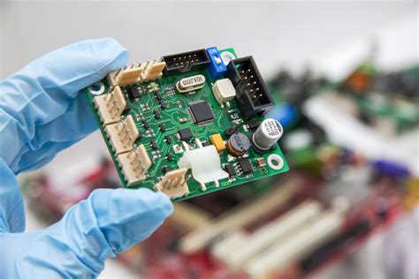
Understanding the PCB Assembly Process
Before diving into the preparation steps, it’s important to have a basic understanding of the PCB assembly process. The process typically involves the following steps:
-
Solder Paste Application: Solder paste, a mixture of tiny solder particles and flux, is applied to the PCB pads where components will be placed.
-
Component Placement: Electronic components are placed onto the PCB using automated pick-and-place machines or manual placement methods.
-
Reflow Soldering: The PCB with the placed components is passed through a reflow oven, where the solder paste melts and forms electrical connections between the components and the PCB pads.
-
Inspection and Testing: The assembled PCB undergoes visual inspection and electrical testing to ensure proper functionality and quality.
Preparing the PCB Design
The first step in preparing for PCB assembly is to ensure that the PCB design is optimized for manufacturability and assembly. Here are some key considerations:
Component Selection and Placement
- Choose components that are readily available and have standardized packages to avoid sourcing issues and assembly challenges.
- Consider the component size, pitch, and orientation to ensure compatibility with the assembly process and equipment.
- Place components in a logical and accessible manner, allowing for efficient placement and soldering.
- Adhere to the manufacturer’s recommended land patterns and footprints for each component.
PCB Layout and Routing
- Follow the recommended PCB design guidelines, such as minimum trace width, spacing, and clearances, to ensure reliable electrical connections and prevent manufacturing issues.
- Route traces efficiently to minimize the PCB size and reduce the overall assembly complexity.
- Consider the use of vias, both through-hole and blind/buried, to optimize the PCB layout and improve signal integrity.
- Incorporate proper grounding and shielding techniques to minimize electromagnetic interference (EMI) and ensure signal integrity.
Design for Manufacturing (DFM)
- Perform a DFM analysis to identify and address any potential manufacturing issues early in the design stage.
- Consider the limitations and capabilities of the PCB fabrication and assembly processes, such as minimum hole sizes, pad sizes, and component spacing.
- Incorporate fiducial markers and alignment features to aid in the accurate placement of components during assembly.
- Include testability features, such as test points and boundary scan, to facilitate testing and debugging of the assembled PCB.

Preparing the Bill of Materials (BOM)
The Bill of Materials (BOM) is a critical document that lists all the components required for the PCB assembly. A well-prepared BOM ensures that the correct components are procured and available for assembly. Consider the following when preparing the BOM:
Component Information
- Include detailed information for each component, such as the manufacturer part number, description, package type, and quantity required.
- Specify any alternative or substitute components that can be used in case of availability issues.
- Provide the component datasheets and any relevant technical specifications to ensure accurate component selection and handling.
Procurement and Lead Times
- Review the component availability and lead times to ensure timely procurement and avoid delays in the assembly process.
- Consider the minimum order quantities (MOQs) and any special handling or storage requirements for the components.
- Establish a reliable supply chain and maintain good relationships with component suppliers to ensure a steady flow of components.
BOM Formatting and Organization
- Use a standardized BOM format that is compatible with the assembly provider’s systems and processes.
- Organize the BOM in a logical manner, grouping components by type, value, or reference designator for easy reference and tracking.
- Include version control and revision history to track any changes made to the BOM throughout the project lifecycle.

Preparing the Assembly Documentation
In addition to the PCB design files and BOM, several other documents are crucial for a successful PCB assembly process. These include:
Assembly Drawings
- Provide clear and detailed assembly drawings that specify the component placement, orientation, and any special assembly instructions.
- Include dimensions, tolerances, and any critical assembly features, such as connector orientations or heat sink placement.
- Use standard drawing formats, such as Gerber or ODB++, that are compatible with the assembly provider’s systems.
Solder Paste Stencil Design
- If using surface mount components, provide a solder paste stencil design that defines the aperture sizes and locations for solder paste application.
- Ensure that the stencil design is aligned with the PCB layout and consider any specific requirements, such as solder paste thickness or stencil material.
Assembly Process Instructions
- Provide detailed instructions for the assembly process, including any specific requirements for component placement, soldering profiles, or inspection criteria.
- Specify any special handling or storage requirements for sensitive components, such as moisture-sensitive devices (MSDs) or electrostatic discharge (ESD) sensitive components.
- Include any necessary quality control measures, such as visual inspection criteria or electrical testing requirements.

Communicating with the Assembly Provider
Effective communication with the PCB assembly provider is essential for a smooth and successful assembly process. Consider the following:
Defining Project Requirements
- Clearly communicate the project requirements, including the PCB quantity, lead time, and any specific quality or certification requirements.
- Discuss any potential challenges or constraints, such as component availability or tight tolerances, and work collaboratively to find solutions.
Reviewing and Approving Files
- Provide all the necessary design files, BOM, and assembly documentation to the assembly provider for review and verification.
- Respond promptly to any questions or clarifications requested by the assembly provider to avoid delays in the assembly process.
- Review and approve any modifications or suggestions made by the assembly provider to ensure compatibility with their processes and equipment.
Establishing a Communication Channel
- Designate a primary point of contact within your organization to communicate with the assembly provider throughout the project.
- Establish a regular communication schedule, such as weekly status updates or milestone reviews, to keep track of the project progress and address any issues promptly.
- Use collaborative tools, such as project management software or shared file repositories, to facilitate effective communication and document sharing.
Preparing for Assembly Logistics
Once the PCB design, BOM, and assembly documentation are ready, it’s important to consider the logistical aspects of the assembly process:
Component Procurement and Inventory Management
- Procure the necessary components based on the BOM and ensure their availability for the assembly process.
- Implement an inventory management system to track component quantities, locations, and expiration dates, especially for components with limited shelf life.
- Consider consignment or vendor-managed inventory arrangements with the assembly provider to streamline the component supply chain.
Shipping and Packaging
- Determine the shipping method and packaging requirements for the PCB panels and components, considering factors such as electrostatic discharge (ESD) protection and moisture sensitivity.
- Label and package the components and PCB panels accurately, including any necessary documentation or certificates of conformance (CoCs).
- Coordinate the shipping schedule with the assembly provider to ensure timely delivery and minimize any delays.
Quality Control and Inspection
- Establish a quality control plan that defines the inspection criteria and testing requirements for the assembled PCBs.
- Discuss the quality control measures with the assembly provider and agree on the acceptance criteria and any necessary corrective actions.
- Consider implementing statistical process control (SPC) techniques to monitor and control the assembly process quality.
Frequently Asked Questions (FAQ)
-
What is the importance of a well-prepared BOM in PCB assembly?
A well-prepared BOM is crucial for ensuring that the correct components are procured and available for the assembly process. It should include detailed information for each component, specify alternative components if needed, and be organized in a logical manner. A comprehensive BOM helps avoid delays and ensures a smooth assembly process. -
How can I optimize my PCB design for manufacturability and assembly?
To optimize your PCB design for manufacturability and assembly, consider factors such as component selection and placement, PCB layout and routing, and design for manufacturing (DFM) principles. Choose readily available components, follow recommended design guidelines, and incorporate features that aid in the assembly process, such as fiducial markers and testability features. -
What are the key documents required for PCB assembly?
The key documents required for PCB assembly include the PCB design files (such as Gerber files), the Bill of Materials (BOM), assembly drawings, solder paste stencil design (for surface mount components), and assembly process instructions. These documents provide the necessary information for the assembly provider to accurately and efficiently assemble the PCBs. -
How can I ensure effective communication with the PCB assembly provider?
Effective communication with the PCB assembly provider involves clearly defining project requirements, promptly reviewing and approving files, and establishing a regular communication channel. Designate a primary point of contact within your organization, use collaborative tools for document sharing, and maintain open lines of communication throughout the project to address any issues or concerns. -
What are some logistical considerations for PCB assembly?
Logistical considerations for PCB assembly include component procurement and inventory management, shipping and packaging, and quality control and inspection. Ensure timely procurement of components, implement an inventory management system, determine appropriate shipping methods and packaging requirements, and establish a quality control plan with agreed-upon acceptance criteria and corrective actions.
| Aspect | Key Considerations |
|---|---|
| PCB Design Preparation | – Component selection and placement – PCB layout and routing – Design for manufacturing (DFM) – Testability features |
| Bill of Materials (BOM) | – Detailed component information – Procurement and lead times – BOM formatting and organization |
| Assembly Documentation | – Assembly drawings – Solder paste stencil design – Assembly process instructions |
| Communication | – Defining project requirements – Reviewing and approving files – Establishing a communication channel |
| Assembly Logistics | – Component procurement and inventory management – Shipping and packaging – Quality control and inspection |
By thoroughly preparing these aspects before PCB assembly, you can ensure a smooth and efficient assembly process, resulting in high-quality and reliable electronic products. Effective communication, attention to detail, and collaboration with the assembly provider are key to successful PCB assembly.


Leave a Reply