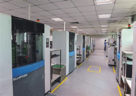
Types of PCB Equipment
PCB Design Software
The first step in creating a PCB is designing the circuit layout using specialized software. Some popular PCB design software include:
- Altium Designer
- KiCad
- Eagle
- OrCAD
These software packages allow engineers to create detailed schematics, define component placement, and route connections between components. They also provide tools for simulating and testing the circuit before fabrication.
PCB Fabrication Equipment
Once the design is finalized, the next step is to fabricate the physical PCB. This process involves several stages, each requiring specific equipment.
PCB Printing Equipment
- Screen Printing Machines
- Used for applying solder paste and other materials onto the PCB surface
- Can print fine details and handle a variety of materials
-
Examples: MPM Accela, DEK Horizon
-
Inkjet Printers
- Used for printing conductive inks and other functional materials
- Offer high precision and flexibility in material deposition
- Examples: Nano Dimension DragonFly, Optomec Aerosol Jet
Etching Equipment
- Chemical Etching Machines
- Use chemical solutions to remove unwanted copper from the PCB surface
- Provide high accuracy and can handle complex designs
-
Examples: Chemcut Etching Systems, WISE CTS-30
-
Plasma Etching Machines
- Use plasma to etch away unwanted materials from the PCB surface
- Offer high precision and can handle a wide range of materials
- Examples: Nordson MARCH AP-1000, Diener electronic Nano
Drilling Equipment
- CNC Drilling Machines
- Used for drilling holes in the PCB for component placement and vias
- Offer high speed and precision drilling capabilities
-
Examples: Excellon Automation M-Series, Schmoll Maschinen MX-Series
-
Laser Drilling Machines
- Use lasers to drill micro-vias and other small features
- Provide high accuracy and can handle delicate materials
- Examples: ESI CapStone, Mitsubishi Electric ML605GTW
PCB Assembly Equipment
After the PCB is fabricated, components must be placed and soldered onto the board. This process involves several types of equipment.
Pick-and-Place Machines
- High-Speed Pick-and-Place Machines
- Used for placing surface mount components onto the PCB
- Offer high speed and accuracy in component placement
-
Examples: Fuji NXT III, Panasonic NPM-W2
-
Multi-Function Pick-and-Place Machines
- Capable of placing a wide range of component sizes and types
- Provide flexibility and can handle mixed-technology assemblies
- Examples: Juki RS-1R, Yamaha YSM20R
Soldering Equipment
- Reflow Soldering Ovens
- Used for soldering surface mount components onto the PCB
- Provide precise temperature control and even heat distribution
-
Examples: BTU Pyramax, Heller 1913 MK5
-
Wave Soldering Machines
- Used for soldering through-hole components onto the PCB
- Offer high-volume soldering capabilities and can handle large components
-
Examples: Electrovert VectraElite, ERSA POWERFLOW
-
Selective Soldering Machines
- Used for soldering specific areas or components on the PCB
- Provide precision and flexibility in the soldering process
- Examples: Pillarhouse Pilot, EBSO SPA-400
Inspection Equipment
- Automated Optical Inspection (AOI) Systems
- Used for inspecting the PCB for defects and component placement accuracy
- Provide high-speed, non-contact inspection capabilities
-
Examples: Koh Young aSPIre3, Mirtec MV-6 OMNI
-
X-Ray Inspection Systems
- Used for inspecting solder joints and internal structures of the PCB
- Offer non-destructive testing and can detect hidden defects
- Examples: Nordson DAGE Quadra 5, Yxlon Cheetah EVO
Advancements in PCB Equipment Technology
As electronic devices become more complex and miniaturized, PCB equipment must evolve to keep pace with these advancements. Some notable developments in PCB equipment technology include:
- 3D Printing for PCBs
- Allows for the creation of complex, three-dimensional PCB structures
- Enables the integration of electronic components within the PCB itself
-
Examples: Nano Dimension DragonFly, Optomec Aerosol Jet
-
Artificial Intelligence (AI) in PCB Assembly
- Uses machine learning algorithms to optimize component placement and routing
- Improves efficiency and reduces the risk of errors in the assembly process
-
Examples: Cogiscan TTC, Koh Young KSMART
-
Robotic Process Automation (RPA)
- Automates repetitive tasks in the PCB assembly process
- Enhances productivity and reduces the need for manual labor
- Examples: Universal Robots UR5, FANUC CRX-10iA

Choosing the Right PCB Equipment
When selecting PCB equipment for your assembly and fabrication needs, consider the following factors:
- Production Volume
- Choose equipment that can handle your expected production volume efficiently
-
Consider scalability for future growth
-
Complexity of PCB Designs
- Ensure the equipment can accommodate the complexity of your PCB designs
-
Look for machines with high precision and flexibility
-
Budget and Return on Investment (ROI)
- Balance your budget with the long-term benefits of the equipment
-
Consider the potential for increased productivity and reduced labor costs
-
Integration with Existing Systems
- Ensure the new equipment can integrate seamlessly with your existing systems and processes
- Look for machines with compatible software and communication protocols

Frequently Asked Questions (FAQ)
- What is the difference between through-hole and surface mount components?
-
Through-hole components have leads that are inserted into holes drilled in the PCB, while surface mount components are placed directly on the surface of the PCB.
-
How does solder paste differ from traditional soldering?
-
Solder paste is a mixture of tiny solder particles suspended in a flux medium, which is applied to the PCB using a stencil or screen printing process. Traditional soldering involves using a soldering iron to melt and apply solder to specific points on the PCB.
-
What are the advantages of using AOI systems in PCB Inspection?
-
AOI systems provide high-speed, non-contact inspection of PCBs, detecting defects such as missing components, incorrect component placement, and solder bridging. They improve quality control and reduce the risk of defective products reaching the end-user.
-
How can 3D printing technology be used in PCB fabrication?
-
3D printing technology allows for the creation of complex, three-dimensional PCB structures, enabling the integration of electronic components within the PCB itself. This can lead to more compact and efficient designs, as well as the possibility of creating custom, application-specific PCBs.
-
What role does AI play in PCB assembly?
- AI algorithms can analyze PCB designs and optimize component placement and routing for improved efficiency and reduced errors. Machine learning can also be used to monitor the assembly process in real-time, detecting anomalies and predicting potential issues before they occur.

Conclusion
PCB assembly and fabrication equipment plays a crucial role in the creation of modern electronic devices. From design software and printing machines to pick-and-place systems and inspection equipment, each stage of the PCB manufacturing process relies on specialized tools to ensure precision, reliability, and efficiency. As technology continues to advance, PCB equipment must evolve to keep pace, incorporating new technologies such as 3D printing, AI, and RPA to meet the ever-growing demands of the electronics industry. By understanding the various types of PCB equipment available and considering factors such as production volume, design complexity, budget, and integration, manufacturers can select the most appropriate tools for their specific needs, ensuring the successful creation of high-quality PCBs for a wide range of applications.


Leave a Reply