Introduction to KiCad
KiCad is a free and open-source electronic design automation (EDA) software suite that enables users to design professional-grade printed circuit boards (PCBs) from scratch. It offers a complete set of tools for schematic capture, PCB layout, and generation of manufacturing files. In this comprehensive KiCad Tutorial, we will guide you through the process of creating a simple PCB project, covering all the essential steps and features.
What is KiCad?
KiCad is a cross-platform EDA software that runs on Windows, macOS, and Linux. It consists of several integrated tools that work together to facilitate the PCB design process:
- Eeschema: Schematic capture editor
- Pcbnew: PCB layout editor
- GerbView: Gerber viewer
- Cvpcb: Footprint selector
- PcbCalculator: PCB Calculator
Why Use KiCad?
There are several reasons why KiCad is a popular choice among electronics enthusiasts and professionals alike:
- Free and open-source: KiCad is available at no cost and allows users to access and modify the source code.
- Cross-platform compatibility: KiCad runs on all major operating systems, ensuring a consistent user experience across different platforms.
- Extensive component libraries: KiCad comes with a vast collection of component libraries, and users can also create custom libraries or import them from various sources.
- Active community support: KiCad has a thriving community of users and developers who contribute to its development, provide support, and share resources.
Getting Started with KiCad
Installing KiCad
To begin using KiCad, you first need to install it on your computer. Follow these steps:
- Visit the official KiCad website: https://www.kicad.org/
- Navigate to the “Download” section and select the appropriate version for your operating system.
- Download the installer and run it, following the on-screen instructions.
- Once the installation is complete, launch KiCad from your applications or start menu.
Creating a New Project
To create a new project in KiCad, follow these steps:
- Open KiCad and click on “File” > “New Project” or press “Ctrl+N”.
- Choose a location for your project and give it a name.
- Click “Save” to create the project folder and files.
Navigating the KiCad Interface
Upon opening KiCad, you will see the main window, which consists of several sections:
- Project tree: Displays the files and folders associated with your project.
- Main toolbar: Provides quick access to frequently used tools and commands.
- Schematic editor: Opens the Eeschema tool for schematic capture.
- PCB layout editor: Opens the Pcbnew tool for PCB layout design.
- Footprint selector: Opens the Cvpcb tool for assigning footprints to components.

Designing the Schematic
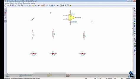
Creating a Schematic in Eeschema
To create a schematic in KiCad, follow these steps:
- Double-click on the “Schematic layout editor” icon in the project tree or click on the “Eeschema” button in the main toolbar.
- The Eeschema window will open, displaying a blank schematic sheet.
- Use the toolbar buttons or hotkeys to place components, draw wires, and add labels and annotations.
- To search for a specific component, press “A” to open the component selector, type the component name or keywords, and double-click on the desired component to place it on the schematic.
- Connect the components using the “Place wire” tool or by pressing “W”.
- Assign unique reference designators to each component by right-clicking on the component and selecting “Annotate”.
- Perform an electrical rules check (ERC) by clicking on the “Perform electrical rules check” button or pressing “E”. This will validate the schematic for any errors or warnings.
Assigning Footprints in Cvpcb
Once you have completed the schematic, you need to assign footprints to each component. Footprints define the physical dimensions and pad layout of the components on the PCB. To assign footprints, follow these steps:
- Click on the “Assign component footprints” button in the Eeschema toolbar or press “F”.
- The Cvpcb window will open, displaying the list of components in your schematic.
- For each component, select the appropriate footprint from the available libraries.
- If a suitable footprint is not available, you can create a custom footprint in the Footprint Editor.
- Once you have assigned footprints to all components, save the changes and close Cvpcb.

Designing the PCB Layout
Creating a PCB in Pcbnew
With the schematic complete and footprints assigned, you can now proceed to design the PCB layout in Pcbnew. Follow these steps:
- Click on the “PCB layout editor” button in the main KiCad window or double-click on the “.kicad_pcb” file in the project tree.
- The Pcbnew window will open, displaying the components and their footprints arranged on the board.
- Use the toolbar buttons or hotkeys to move and rotate components, route traces, and define the board outline.
- To route traces between pads, use the “Route tracks” tool or press “X”.
- Define the board stackup and design rules by clicking on “File” > “Board Setup”.
- Perform a design rules check (DRC) by clicking on the “Perform design rules check” button or pressing “D”. This will validate the PCB layout for any violations of the specified design rules.
Adding Copper Pours and Text
To enhance the functionality and aesthetics of your PCB, you can add copper pours and text. Copper pours are solid areas of copper that provide shielding, power distribution, or heat dissipation. Text can be used for labeling components, providing instructions, or adding your logo. Follow these steps:
- To add a copper pour, click on the “Add filled zones” button or press “U”. Define the outline of the pour area and specify the net name and other properties.
- To add text, click on the “Add text” button or press “T”. Type the desired text, adjust its properties, and place it on the PCB.

Generating Manufacturing Files
Once your PCB layout is complete and has passed the DRC, you can generate the manufacturing files required for production. These files include Gerber files, drill files, and assembly drawings. Follow these steps:
- Click on “File” > “Plot” or press “P” to open the plot dialog.
- Select the layers you want to plot, such as copper layers, silkscreen, and solder mask.
- Choose the output directory and file format (usually Gerber).
- Click “Plot” to generate the Gerber files.
- To generate the drill files, click on “Generate Drill Files” in the plot dialog. Specify the output directory and file format.
- Open the generated files in GerbView to verify their correctness.
FAQs
1. Is KiCad suitable for beginners?
Yes, KiCad is an excellent choice for beginners who want to learn PCB design. It offers a user-friendly interface, extensive documentation, and a supportive community that provides help and resources.
2. Can I create complex PCBs with KiCad?
Absolutely. KiCad is a powerful tool that can handle both simple and complex PCB designs. It offers advanced features such as hierarchical schematic design, multi-sheet projects, and scripting capabilities.
3. Are there any limitations on board size or layer count in KiCad?
KiCad does not impose any hard limits on board size or layer count. However, the practical limitations depend on your computer’s hardware and the complexity of your design.
4. Can I import designs from other EDA software into KiCad?
Yes, KiCad supports importing designs from various formats, including Eagle, Altium, and OrCAD. You can use the “File” > “Import” menu to bring in schematic and PCB Files from other tools.
5. How can I learn more about KiCad and PCB design?
There are numerous resources available to help you learn KiCad and PCB design:
- Official KiCad documentation: https://docs.kicad.org/
- KiCad forums: https://forum.kicad.info/
- YouTube tutorials and video courses
- PCB design blogs and websites
- Books on PCB design and KiCad
| Feature | Description |
|---|---|
| Cross-platform | Runs on Windows, macOS, and Linux |
| Free and open-source | Available at no cost with modifiable source code |
| Schematic capture | Create and edit electronic schematics |
| PCB layout | Design and route printed circuit boards |
| Component libraries | Extensive collection of pre-made and custom components |
| Footprint editor | Create and edit component footprints |
| 3D viewer | Visualize the PCB in 3D |
| Manufacturing output | Generate Gerber, drill, and assembly files |
Conclusion
In this comprehensive KiCad tutorial, we have covered the essential steps and features required to design a PCB from scratch. By following this guide, you should now have a solid understanding of how to create a schematic, assign footprints, design the PCB layout, and generate manufacturing files.
KiCad is a powerful and versatile EDA software that offers a complete solution for PCB design. Its free and open-source nature, combined with its active community and extensive resources, make it an attractive choice for both beginners and experienced designers.
As you continue to explore KiCad and PCB design, remember to consult the official documentation, participate in the community forums, and practice your skills with various projects. With dedication and practice, you will soon be creating professional-grade PCBs with ease.


Leave a Reply