Introduction to PCB fabrication
Printed Circuit Boards (PCBs) are the backbone of modern electronics. They provide a platform for mounting and interconnecting electronic components, allowing for the creation of complex circuits in a compact and efficient manner. While PCBs are typically manufactured in large-scale industrial facilities, it is possible to create them at home with the right tools and techniques. In this article, we will explore the process of PCB fabrication at home, covering everything from designing the circuit to etching and drilling the board.
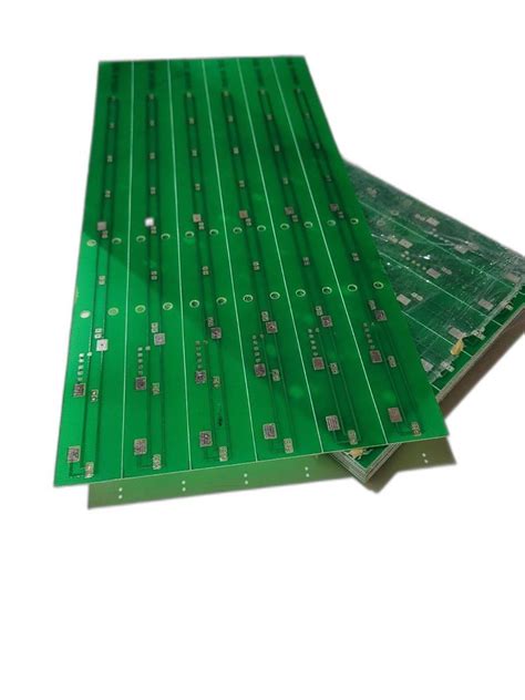
What is a PCB?
A PCB is a thin board made of insulating material, such as fiberglass or epoxy resin, with conductive tracks printed on one or both sides. These tracks, also known as traces, connect the various components of the circuit, allowing for the flow of electrical signals. PCBs can be single-sided, with traces on only one side of the board, or double-sided, with traces on both sides. They can also have multiple layers, with traces sandwiched between insulating layers.

Advantages of Making PCBs at Home
While it may seem daunting at first, making PCBs at home has several advantages:
-
Cost Savings: Commercial PCB fabrication services can be expensive, especially for small batches or prototypes. Making your own PCBs at home can significantly reduce costs.
-
Rapid Prototyping: When designing circuits, it’s often necessary to create multiple iterations before arriving at the final design. Making PCBs at home allows for quick turnaround times between design revisions.
-
Customization: Home PCB fabrication allows for greater control over the design and specifications of the board, enabling the creation of highly customized circuits.
-
Learning Opportunity: The process of making PCBs at home provides a hands-on learning experience, helping to better understand the principles of electronics and circuit design.

Tools and Materials Required
To make PCBs at home, you will need the following tools and materials:
| Tool/Material | Description |
|---|---|
| PCB Design Software | Software for designing the circuit schematic and PCB layout |
| Laser Printer | For printing the PCB artwork onto transfer paper |
| Transfer Paper | Special paper for transferring the PCB artwork to the copper board |
| Copper Clad Board | A board with a thin layer of copper on one or both sides |
| Etching Solution | Chemical solution for removing unwanted copper from the board |
| Etching Tank | Container for holding the etching solution and PCB during etching |
| Drill | For drilling holes in the PCB for component leads |
| Soldering Iron | For soldering components to the PCB |
| Safety Equipment | Gloves, goggles, and a well-ventilated work area |

Step-by-Step Guide to Making PCBs at Home
Step 1: Design the Circuit
The first step in making a PCB is to design the circuit. This involves creating a schematic diagram that shows the connections between the various components. There are many software tools available for circuit design, ranging from simple freeware to professional-grade software. Some popular options include:
- KiCad
- Eagle
- EasyEDA
- Altium Designer
When designing the circuit, consider factors such as component placement, trace width, and power requirements. It’s also important to adhere to design rules and guidelines to ensure the manufacturability and reliability of the PCB.
Step 2: Create the PCB Layout
Once the schematic is complete, the next step is to create the PCB layout. This involves arranging the components on the board and routing the traces between them. PCB design software typically has tools for automating this process, but it’s important to review and refine the layout manually to ensure optimal performance.
When creating the PCB layout, consider the following:
- Component placement for optimal signal integrity and ease of assembly
- Trace width and spacing to minimize crosstalk and electromagnetic interference
- Ground planes and power distribution for stable power delivery
- Thermal management for heat-generating components
Step 3: Print the PCB Artwork
With the PCB layout complete, the next step is to print the artwork onto transfer paper. This involves exporting the PCB layout as a high-resolution image file, such as a PDF or PNG, and printing it onto the transfer paper using a laser printer.
It’s important to use a laser printer rather than an inkjet printer, as the toner from a laser printer is more heat-resistant and will transfer better to the copper board. Also, ensure that the artwork is printed at the correct scale and with high contrast for best results.
Step 4: Transfer the Artwork to the Copper Board
To transfer the artwork to the copper board, follow these steps:
-
Clean the copper board with steel wool or fine sandpaper to remove any oxidation and ensure good adhesion of the toner.
-
Place the transfer paper with the printed side facing the copper board and secure it in place with heat-resistant tape.
-
Use a clothes iron set to high heat (without steam) to press the transfer paper onto the copper board. Apply firm, even pressure for several minutes, ensuring that the entire artwork is transferred.
-
Allow the board to cool, then carefully peel off the transfer paper. The toner artwork should now be adhered to the copper board.
Step 5: Etch the PCB
With the artwork transferred to the copper board, the next step is to etch away the unwanted copper. This is typically done using a chemical etching solution, such as ferric chloride or ammonium persulfate.
To etch the PCB, follow these steps:
-
Put on protective gloves and goggles, and work in a well-ventilated area.
-
Place the PCB in the etching tank and pour in the etching solution. The solution should cover the entire board.
-
Agitate the solution periodically to ensure even etching. The etching process can take anywhere from a few minutes to an hour, depending on the strength of the solution and the size of the board.
-
Once etching is complete, remove the board from the solution and rinse it thoroughly with water.
-
Remove the remaining toner artwork using acetone or a dedicated PCB cleaner.
Step 6: Drill Holes and Solder Components
With the PCB etched, the final steps are to drill holes for component leads and solder the components in place.
To drill holes, use a drill with a small bit (typically 0.8mm to 1.5mm) and carefully drill through the center of each pad. It’s important to use a drill stand or a steady hand to ensure the holes are perpendicular to the board.
To solder components, follow these steps:
-
Place the component leads through the corresponding holes in the PCB.
-
Apply heat to the pad using a soldering iron, then apply solder to the joint. The solder should flow evenly around the lead and pad.
-
Trim any excess lead length with wire cutters.
-
Repeat for all components until the board is fully assembled.
Tips for Successful PCB Fabrication
- Start with simple designs and work your way up to more complex circuits as you gain experience.
- Always double-check the PCB layout before printing the artwork to catch any errors or design rule violations.
- Use high-quality materials, such as fresh etching solution and clean copper boards, for best results.
- Be patient and take your time during the etching process to ensure even and complete copper removal.
- Practice good soldering technique to create reliable joints and avoid damaging components.
Frequently Asked Questions (FAQ)
1. Can I make multi-layer PCBs at home?
While it is possible to make multi-layer PCBs at home, it is significantly more challenging than making single or double-sided boards. It requires precise alignment of the layers and specialized equipment for laminating and drilling. For most hobbyists and small-scale projects, single or double-sided PCBs are sufficient.
2. What safety precautions should I take when making PCBs?
Making PCBs involves the use of chemicals and heat, so it’s important to take appropriate safety precautions. Always wear gloves and goggles when handling etching solution, and work in a well-ventilated area. When soldering, use a fume extractor or work in a ventilated area to avoid inhaling solder fumes. Also, be careful when handling hot objects, such as the soldering iron or freshly etched boards.
3. Can I use inkjet printer instead of laser printer for PCB artwork?
While it is possible to use an inkjet printer for PCB artwork, it is not recommended. Inkjet printer ink is not as heat-resistant as laser printer toner, and may not transfer well to the copper board. Also, inkjet printers typically have lower resolution than laser printers, which can result in less precise artwork.
4. How do I choose the right etching solution?
The two most common etching solutions for home PCB fabrication are ferric chloride and ammonium persulfate. Ferric chloride is easier to use and more readily available, but it can stain surfaces and clothing. Ammonium persulfate is less messy but requires more careful handling and storage. The choice ultimately depends on personal preference and availability.
5. Can I reuse the etching solution?
Etching solution can be reused multiple times, but it will become less effective with each use as the copper content increases. To extend the life of the solution, you can regenerate it by adding more of the active ingredient (ferric chloride or ammonium persulfate) and aerating it to oxidize the dissolved copper. However, it’s important to properly dispose of the solution when it becomes too saturated with copper, as it can be harmful to the environment.
Conclusion
Making PCBs at home is a rewarding and educational process that allows for greater control over the design and fabrication of electronic circuits. By following the steps outlined in this article and practicing good safety and technique, hobbyists and small-scale designers can create professional-quality PCBs without the need for expensive equipment or services.
As with any skill, making PCBs requires practice and patience. Start with simple designs and work your way up to more complex circuits as you gain experience. With time and effort, you’ll be able to create custom PCBs for all your electronic projects, opening up a world of possibilities for innovation and creativity.


Leave a Reply