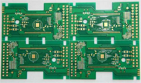
What is PCB etching?
PCB etching is the process of removing unwanted copper from a printed circuit board (PCB) to create the desired electrical connections. The process involves applying a resist layer to the copper surface of the PCB, exposing it to light through a photomask, and then chemically etching away the exposed copper. This leaves behind the desired copper traces that form the electrical connections on the PCB.
PCB etching is a crucial step in the manufacturing process of PCBs, as it allows for the creation of complex and precise electrical circuits. The process can be done manually or through automated machines, depending on the scale of production and the complexity of the design.
Why is PCB Etching Important?
PCB etching is important for several reasons:
-
Creates Electrical Connections: PCB etching allows for the creation of the desired electrical connections on the PCB. Without etching, the copper layer on the PCB would remain intact, and no electrical circuits could be formed.
-
Enables Complex Designs: PCB etching enables the creation of complex and precise electrical circuits. This is particularly important for modern electronics, which often require high-density PCBs with fine pitch traces.
-
Ensures Reliability: Properly etched PCBs are more reliable than those with poorly etched or incomplete circuits. Incomplete or incorrect etching can lead to short circuits, open circuits, or other issues that can affect the performance and reliability of the final product.
-
Cost-effective: PCB etching is a cost-effective way to create electrical circuits on a PCB. Alternative methods, such as milling or drilling, can be more expensive and time-consuming.

PCB Etching Process Steps
The PCB etching process involves several steps, which are outlined below:
Step 1: Design the PCB
The first step in the PCB etching process is to design the PCB. This involves creating a schematic diagram of the electrical circuit and then laying out the physical design of the PCB using CAD software. The design should include the placement of components, the routing of traces, and any other necessary features.
Step 2: Print the Photomask
Once the PCB design is complete, the next step is to print the photomask. The photomask is a transparent film with the PCB design printed on it in black ink. The photomask is used to selectively expose the photoresist layer on the PCB to light.
Step 3: Apply the Photoresist
The next step is to apply the photoresist layer to the copper surface of the PCB. The photoresist is a light-sensitive material that hardens when exposed to light. There are two types of photoresist: positive and negative. Positive photoresist becomes soluble when exposed to light, while negative photoresist becomes insoluble.
The photoresist is typically applied by spin coating, where the PCB is placed on a spinning platform and the photoresist is poured onto the center of the board. The spinning action spreads the photoresist evenly across the surface of the PCB.
Step 4: Expose the Photoresist
Once the photoresist is applied, the next step is to expose it to light through the photomask. The photomask is placed on top of the PCB, and the assembly is placed in a UV exposure unit. The UV light passes through the transparent areas of the photomask and exposes the photoresist underneath.
The exposure time depends on the type of photoresist and the intensity of the UV light. Overexposure can cause the photoresist to become too hard, while underexposure can cause it to become too soft.
Step 5: Develop the Photoresist
After exposure, the next step is to develop the photoresist. The PCB is immersed in a developer solution, which selectively dissolves the exposed (positive) or unexposed (negative) areas of the photoresist.
The development time depends on the type of photoresist and the strength of the developer solution. Overdevelopment can cause the photoresist to be completely removed, while underdevelopment can leave residual photoresist on the PCB.
Step 6: Etch the PCB
Once the photoresist is developed, the next step is to etch the PCB. The PCB is immersed in an etching solution, which chemically removes the exposed copper. The most common etching solutions are ferric chloride and ammonium persulfate.
The etching time depends on the strength of the etching solution and the thickness of the copper layer. Overetching can cause the copper traces to become too thin or even disappear entirely, while underetching can leave unwanted copper on the PCB.
Step 7: Remove the Photoresist
After etching, the final step is to remove the remaining photoresist from the PCB. This is typically done using a stripping solution, which chemically dissolves the photoresist.
The stripping time depends on the type of photoresist and the strength of the stripping solution. Overstripping can cause damage to the copper traces, while understripping can leave residual photoresist on the PCB.

PCB Etching Techniques
There are several techniques that can be used for PCB etching, each with its own advantages and disadvantages. The most common techniques are:
Chemical Etching
Chemical etching is the most common technique for PCB etching. It involves immersing the PCB in an etching solution, which chemically removes the exposed copper. The most common etching solutions are ferric chloride and ammonium persulfate.
Advantages:
– Relatively simple and inexpensive
– Can produce fine pitch traces
– Can be done manually or with automated machines
Disadvantages:
– Requires the use of hazardous chemicals
– Can be messy and time-consuming
– Requires proper ventilation and safety equipment
Plasma Etching
Plasma etching is a dry etching technique that uses a plasma to remove the exposed copper. The PCB is placed in a vacuum chamber, and a plasma is generated using a high-frequency electric field. The plasma reacts with the exposed copper, converting it into a volatile compound that is removed from the chamber.
Advantages:
– Produces very fine pitch traces
– Can etch through thick copper layers
– Does not require the use of hazardous chemicals
Disadvantages:
– Requires specialized equipment
– Can be expensive
– May require multiple etching steps
Laser Etching
Laser etching uses a high-powered laser to remove the exposed copper. The laser beam is focused onto the PCB surface, and the copper is vaporized or ablated away.
Advantages:
– Can produce very fine pitch traces
– Does not require the use of hazardous chemicals
– Can be very fast and accurate
Disadvantages:
– Requires specialized equipment
– Can be expensive
– May require multiple etching steps

PCB Etching Equipment
To perform PCB etching, several pieces of equipment are required. The most common equipment includes:
Etching Tank
An etching tank is a container that holds the etching solution and the PCB during the etching process. Etching tanks can be made of plastic or glass and come in various sizes depending on the size of the PCBs being etched.
Photomask Printer
A photomask printer is used to print the PCB design onto a transparent film. The most common type of photomask printer is an inkjet printer with special transparency film.
UV Exposure Unit
A UV exposure unit is used to expose the photoresist layer on the PCB to UV light. The most common type of UV exposure unit is a UV lamp with a timer and a vacuum table to hold the PCB and photomask in place.
Spin Coater
A spin coater is used to apply the photoresist layer to the PCB. The PCB is placed on a spinning platform, and the photoresist is poured onto the center of the board. The spinning action spreads the photoresist evenly across the surface of the PCB.
Developing and Stripping Baths
Developing and stripping baths are used to develop the photoresist and remove the remaining photoresist after etching. These baths typically consist of plastic or glass containers filled with the appropriate solutions.
Safety Considerations
PCB etching involves the use of hazardous chemicals and requires proper safety precautions to prevent injury or damage. Some important safety considerations include:
- Wear appropriate personal protective equipment (PPE), including gloves, goggles, and a respirator.
- Work in a well-ventilated area or use a fume hood to prevent inhalation of chemical fumes.
- Properly dispose of used etching solutions and waste materials in accordance with local regulations.
- Store chemicals in properly labeled containers and keep them away from heat and flame.
- Never mix different etching solutions or chemicals, as this can cause dangerous reactions.
Troubleshooting Common PCB Etching Problems
While PCB etching is a relatively straightforward process, several common problems can occur. Some of these problems and their solutions are:
Incomplete Etching
Incomplete etching occurs when the etching solution does not remove all of the exposed copper, leaving behind unwanted copper on the PCB.
Solutions:
– Increase the etching time or the strength of the etching solution.
– Agitate the PCB during etching to ensure even exposure to the etching solution.
– Check the photomask for any defects or areas that may have blocked the UV light.
Overetching
Overetching occurs when the etching solution removes too much copper, causing the traces to become too thin or disappear entirely.
Solutions:
– Reduce the etching time or the strength of the etching solution.
– Monitor the etching process closely and remove the PCB from the etching solution as soon as the copper is completely removed.
– Use a larger trace width in the PCB design to compensate for some overetching.
Poor Adhesion of Photoresist
Poor adhesion of the photoresist can cause the photoresist to lift or peel off during the etching process, resulting in unwanted copper removal.
Solutions:
– Clean the PCB thoroughly before applying the photoresist to remove any dirt, grease, or oxidation.
– Apply the photoresist in a clean, dust-free environment.
– Use a higher quality photoresist or a different application method, such as dip coating or spray coating.
Underexposure or Overexposure of Photoresist
Underexposure of the photoresist can cause the photoresist to be too soft and easily removed during development, while overexposure can cause the photoresist to be too hard and difficult to remove.
Solutions:
– Adjust the exposure time or intensity of the UV light to achieve the proper exposure level.
– Use a step wedge or exposure calculator to determine the optimal exposure time for the specific photoresist and UV light source being used.
– Check the UV light source for any degradation or inconsistencies in output.
FAQs
What is the best etching solution to use for PCB etching?
The best etching solution depends on the specific application and requirements of the PCB. Ferric chloride and ammonium persulfate are the most common etching solutions, but other solutions such as cupric chloride and sodium persulfate can also be used. Factors to consider when choosing an etching solution include the speed of etching, the ability to produce fine pitch traces, and the safety and environmental impact of the solution.
Can I reuse the etching solution?
Etching solutions can be reused multiple times, but their effectiveness will decrease with each use as the copper content increases. It is important to monitor the etching solution and replace it when it becomes too saturated with copper or loses its effectiveness. Proper disposal of used etching solutions is also important to prevent environmental contamination.
How do I know when the etching process is complete?
The etching process is complete when all of the exposed copper has been removed from the PCB. This can be visually inspected by looking for any remaining copper on the PCB surface. It is important to remove the PCB from the etching solution as soon as the copper is completely removed to prevent overetching and damage to the traces.
Can I etch a double-sided PCB using the same process?
Yes, double-sided PCBs can be etched using the same process as single-sided PCBs. However, it is important to ensure that the photomask and photoresist are properly aligned on both sides of the PCB to prevent any misalignment or registration errors. Double-sided PCBs may also require additional processing steps, such as through-hole plating or via drilling, to complete the electrical connections between the two sides.
What safety precautions should I take when etching PCBs?
PCB etching involves the use of hazardous chemicals and requires proper safety precautions to prevent injury or damage. Some important safety considerations include wearing appropriate personal protective equipment (PPE) such as gloves, goggles, and a respirator, working in a well-ventilated area or using a fume hood, properly disposing of used etching solutions and waste materials, storing chemicals in properly labeled containers away from heat and flame, and never mixing different etching solutions or chemicals. It is also important to follow the manufacturer’s instructions and safety data sheets (SDS) for the specific chemicals being used.
Conclusion
PCB etching is a critical process in the manufacturing of printed circuit boards that allows for the creation of complex and precise electrical circuits. The process involves several steps, including designing the PCB, printing the photomask, applying and exposing the photoresist, developing the photoresist, etching the PCB, and removing the remaining photoresist.
There are several techniques that can be used for PCB etching, including chemical etching, plasma etching, and laser etching, each with its own advantages and disadvantages. Proper equipment and safety precautions are also essential for successful PCB etching and to prevent injury or damage.
While PCB etching is a relatively straightforward process, several common problems can occur, such as incomplete etching, overetching, poor adhesion of photoresist, and underexposure or overexposure of photoresist. Troubleshooting these problems requires careful attention to the etching process and adjustments to the etching parameters as needed.
Overall, PCB etching is a critical process that enables the creation of complex and precise electrical circuits for a wide range of applications. By understanding the process steps, techniques, equipment, and safety considerations involved in PCB etching, designers and manufacturers can ensure the successful creation of high-quality PCBs for their products.


Leave a Reply