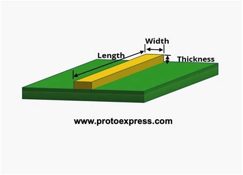
Understanding PCB trace width and Current Capacity
When designing a printed circuit board (PCB), one of the crucial aspects to consider is the trace width and its current-carrying capacity. PCB traces are the copper paths that carry electrical signals and power between components on the board. Determining the appropriate trace width is essential to ensure that the traces can handle the required current without overheating or causing voltage drops, which could lead to system malfunctions or failures.
Factors Affecting PCB Trace Current Capacity
Several factors influence the current-carrying capacity of a PCB trace:
- Trace width: Wider traces can carry more current than narrower traces.
- Copper thickness: Thicker copper layers allow for higher current capacity.
- Temperature rise: The maximum allowable temperature rise limits the current a trace can carry without overheating.
- Ambient temperature: Higher ambient temperatures reduce the current capacity of a trace.
- Trace length: Longer traces have higher resistance, which can cause voltage drops and limit current capacity.
IPC-2152 Standard for Current-Carrying Capacity
The IPC-2152 standard, “Standard for Determining Current-Carrying Capacity in Printed Board Design,” provides guidelines for calculating the current-carrying capacity of PCB traces. This standard takes into account various factors, such as copper thickness, temperature rise, and ambient temperature, to provide accurate current capacity calculations.
According to IPC-2152, the current-carrying capacity of a PCB trace can be calculated using the following equation:
I = k * ΔT^(0.44) * (W * H)^(0.725)
Where:
– I = Current in amps (A)
– ΔT = Temperature rise above ambient in °C
– W = Trace width in mils (1 mil = 0.001 inch)
– H = Copper thickness in mils
– k = Constant (0.048 for external layers, 0.024 for internal layers)
PCB Trace Width Calculation
To determine the appropriate trace width for a given current, you can use the IPC-2152 equation and solve for the trace width (W). However, this process can be time-consuming and prone to errors. Fortunately, there are many online tools and calculators that simplify the process of determining trace widths based on the IPC-2152 standard.
One such tool is the PCB Trace Width Calculator by Multi-CB. This calculator allows you to input the required current, copper thickness, temperature rise, and other parameters to determine the minimum trace width needed for your design.
Example Trace Width Calculation
Let’s consider an example where you need to determine the minimum trace width for a current of 2A, with a copper thickness of 1 oz/ft² (1.4 mils), a temperature rise of 10°C, and an ambient temperature of 25°C.
Using the PCB Trace Width Calculator, we input the following values:
– Current: 2A
– Copper Thickness: 1 oz/ft² (1.4 mils)
– Temperature Rise: 10°C
– Ambient Temperature: 25°C
– Layer: External
The calculator determines that the minimum trace width required for these parameters is approximately 45 mils (1.143 mm).

PCB Trace Current Capacity Tables
While online calculators are convenient for quick trace width determinations, it’s often helpful to have reference tables that provide current capacities for common trace widths and copper thicknesses. These tables allow for quick estimates during the PCB design process.
The following table provides current capacities for various trace widths and copper thicknesses, assuming a temperature rise of 10°C and an ambient temperature of 25°C:
| Trace Width (mils) | 0.5 oz/ft² (0.7 mils) | 1 oz/ft² (1.4 mils) | 2 oz/ft² (2.8 mils) |
|---|---|---|---|
| 10 | 0.5 A | 0.7 A | 1.0 A |
| 20 | 0.8 A | 1.2 A | 1.7 A |
| 30 | 1.1 A | 1.6 A | 2.3 A |
| 40 | 1.4 A | 2.0 A | 2.8 A |
| 50 | 1.7 A | 2.4 A | 3.4 A |
It’s important to note that these values are estimates and may not account for all factors affecting current capacity. Always refer to the IPC-2152 standard and use appropriate calculators for more accurate results.

Frequently Asked Questions (FAQ)
- What happens if I use a trace width that’s too narrow for the required current?
Using a trace width that’s too narrow for the required current can lead to excessive heating, causing the trace to become a fuse and potentially break. This can result in system malfunctions or failures. Always ensure that your trace widths are sufficient for the expected current.
- Can I use thinner copper layers to save on PCB costs?
While using thinner copper layers can reduce PCB Manufacturing Costs, it also reduces the current-carrying capacity of the traces. This means you may need to use wider traces to compensate for the thinner copper, which can take up more space on the PCB. It’s essential to strike a balance between cost and performance when selecting copper thickness.
- How does ambient temperature affect PCB trace current capacity?
Higher ambient temperatures reduce the current-carrying capacity of PCB traces. This is because the trace has less room for temperature rise before reaching its maximum allowable temperature. When designing PCBs for high-temperature environments, it’s crucial to account for the reduced current capacity and adjust trace widths accordingly.
- What is the difference between internal and external copper layers in terms of current capacity?
External copper layers (top and bottom layers) have a higher current-carrying capacity compared to internal layers. This is due to the better heat dissipation on the outer layers, as they are exposed to air. When calculating trace widths, it’s important to use the appropriate constant (k) for internal (0.024) or external (0.048) layers.
- Can I use the same trace width for all signals on my PCB?
Not all signals require the same trace width. Power traces, which carry higher currents, typically require wider traces than signal traces. It’s essential to calculate the appropriate trace width for each signal based on its current requirements. This helps optimize PCB space utilization and ensures reliable performance.

Conclusion
Determining the appropriate PCB trace width and current capacity is crucial for designing reliable and efficient PCBs. By understanding the factors affecting current capacity and using the IPC-2152 standard, designers can ensure that their traces are sufficient for the required currents. Online calculators and reference tables provide quick and easy ways to estimate trace widths during the design process.
By following these guidelines and carefully considering the specific requirements of your PCB design, you can create PCBs that perform well, minimize the risk of failures, and ensure the long-term reliability of your electronic devices.


Leave a Reply