Ceramic printed circuit boards (PCB) provide high performance and reliability for demanding applications like automotive, aerospace, military and high power electronics. The thickness of ceramic PCBs depends on the substrate material and design requirements.
This article discusses common ceramic PCB thickness ranges and the factors influencing thickness selection.
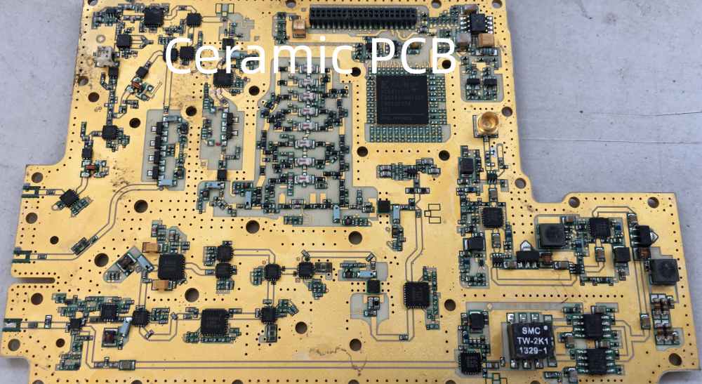
What is Ceramic PCB?
Ceramic PCBs use ceramic materials like aluminum oxide or aluminum nitride as the insulating substrate instead of the standard FR4 material. Ceramic offers:
- High temperature tolerance
- Excellent electrical insulation
- Improved thermal conductivity
- Hermetic sealing ability
- Resistance to humidity and chemicals
These benefits make ceramic PCBs suitable for high frequency, high power and extreme environment applications.
Typical Thickness Range
The thickness of ceramic PCBs generally ranges from 0.25 mm to 3.2 mm (0.010″ to 0.125″).
Some typical thickness options include:
- 0.25 mm
- 0.38 mm
- 0.51 mm
- 0.64 mm
- 1.0 mm
- 1.6 mm
- 2.0 mm
- 2.5 mm
- 3.2 mm
Thinner ceramic PCBs down to 0.1 mm are also possible for lightweight and space constrained applications.
On the higher end, ceramic PCBs up to 6.35 mm (0.25”) are made, albeit less commonly.
So in most cases, ceramic PCB thickness varies from sub-millimeter levels up to 2-3 mm range.
Factors Influencing Thickness
Some key considerations when selecting ceramic PCB thickness include:
Number of Layers
Multilayer ceramic boards with 4-8 layers or more require greater thickness to accommodate multiple conductor and dielectric layers.
Component Heights
Tall components like capacitors and connectors need sufficient thickness to be properly seated. Insufficient thickness results in components extending beyond board surface.
Substrate Strength
For larger boards or those subject to flexing, vibration or impacts, thicker ceramic core provides mechanical robustness.
Thermal Loads
Higher power circuits producing more heat dissipation require thicker ceramic cores like aluminum nitride to spread heat effectively.
Operating Voltage
Thicker dielectric spacing helps manage higher voltages in ceramic PCB layer stackup without dielectric breakdown.
Weight Considerations
In aircraft and space applications, minimum thickness may be preferred to reduce weight despite higher cost.
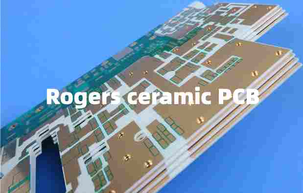
Construction of Thick Ceramic PCBs
Thicker ceramic PCBs above 2 mm are typically constructed by:
Lamination
Laminating separate cured ceramic dielectric layers together under temperature and pressure to form a multilayer board. Allows mixing dielectric materials.
Green Tape Buildup
Stacking and laminating together ceramic green tape layers containing printed conductor patterns. Tapes are cofired to sinter into a single board.
Machining Down
Sintering a thick monolithic ceramic slab and then using diamond grinding to achieve desired thickness. Avoid lamination issues.
Metal Core Substrates
Combining a metal plate like aluminum or copper with direct bonded ceramic dielectric layers. Gives thermal management.
Thin Ceramic PCB Construction
Thin ceramic PCBs below 1 mm thickness are fabricated by:
Dicing Thick Substrates
Taking thicker ceramic plates made by sintering or casting and dicing them down to thinner cuts.
Green Tape Casting
Tape casting ceramic slurries into thin flexible green tapes that can be stacked and laminated.
Microwave Co-fired Ceramics
Printing metal and dielectric layers on ceramic tapes that are cofired into a single thin board.
Advantages of Thinner Ceramic PCBs
Thinner ceramic PCBs offer benefits like:
- Smaller footprint and less weight
- Allows flexible or conformal PCB designs
- Faster heat transfer through thinner dielectric
- Higher production yield with fewer layer lamination issues
- Allows denser vertical interconnections between layers
- Lower material costs
But the thinness decreases mechanical robustness requiring careful handling.
Advantages of Thicker Ceramic PCBs
Increasing ceramic PCB thickness provides advantages like:
- Stronger board physically able to withstand stress
- Spreads heat over larger substrate volume
- Allows higher component heights to be mounted
- Accommodates higher layer count if needed
- Withstands higher voltage isolation requirements
- Can incorporate embedded metal cores for heat sinking
However, thickness limits PCB density and increases thermal resistance through the dielectric.
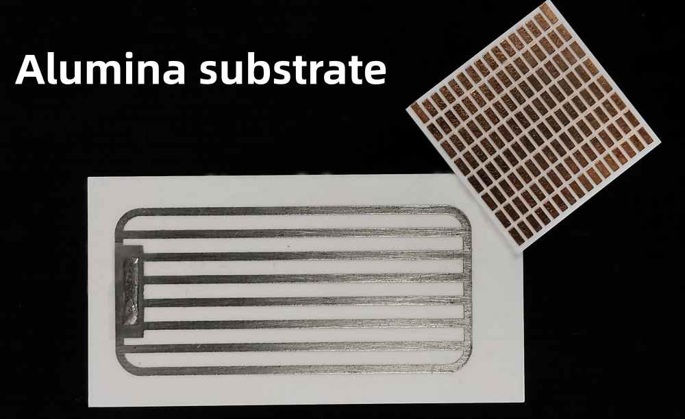
Typical Ceramic Materials Used
Some common ceramic materials used for PCB substrates include:
| Material | Description |
|---|---|
| Alumina (Al2O3) | Most popular. Offers good insulation, thermal conductivity and cost balance. |
| Aluminum Nitride (AlN) | Highest thermal conductivity and heat dissipation. Costly. |
| Beryllium Oxide (BeO) | Excellent thermal conductor but toxicity causes usage restrictions. |
| Silicon Nitride (Si3N4) | Good mechanical strength with moderate thermal conduction. |
| Glass Ceramics | Lower cost but poorer electrical and thermal performance. |
Alumina provides the best all-round performance and cost for most applications. AlN chosen when utmost heat dissipation is critical.
Ceramic PCB vs. FR4 PCB Thickness
FR4 glass epoxy PCBs are commonly produced in thickness from 0.4 mm up to 3.2 mm maximum.
So the thickness range of ceramic PCBs overlaps with FR4 PCBs. But ceramics can go thinner than FR4 for ultra-light boards or ultra-thick for complex layer stacks.
Examples of Ceramic PCB Thickness
Some examples of ceramic PCB thickness used for different applications:
- Consumer electronics – 0.25 mm to 0.64 mm
- Aerospace controls – 1 mm
- Electric vehicle power module – 1.6 mm
- locomotive engine controller – 2.5 mm
- Base station antenna module – 3 mm
- Downhole oil drilling tools – 3.2 mm
FAQs
What is the advantage of thinner PCBs?
Thinner PCBs offer benefits like reduced weight, smaller footprint, flexibility, lowered costs and improved heat dissipation. But compromise on mechanical strength.
Can you bend ceramic PCBs?
Ceramic PCBs have minimal flexibility compared to FR4 boards. But thin ceramic PCBs under 0.5mm can allow limited bending and flexing when required.
Is ceramic PCB fragile?
Ceramics are hard but brittle, susceptible to cracking from impacts or excessive loads. Thin ceramic PCBs are fragile requiring careful handling. Proper mounting schemes improve robustness.
How are components attached to ceramic PCBs?
Soldering, conductive epoxy and direct copper bonding are used to attach components to ceramic PCBs. Standard soldering processes must be adapted for ceramics.
Can you drill holes in ceramic PCB?
Yes, holes can be drilled through ceramic PCBs using diamond coated carbide bits and rigidity enforcing back support to prevent cracking. Laser drilling is also used.
In summary, ceramic PCB thickness typically ranges from 0.25 mm to 3.2 mm, with thinner boards providing miniaturization and thicker boards offering robustness. The specific application requirements ultimately determine the ideal thickness.


Leave a Reply