Alumina (aluminum oxide) PCBs provide superior thermal management and electrical insulation compared to traditional FR4 circuit boards. Alumina PCBs are made using high purity alumina ceramic as the substrate material. This enables thinner boards with improved thermal conductivity and dielectric strength.
Determining the optimal thickness for an alumina PCB depends on the application requirements, manufacturing constraints and design tradeoffs. Below we discuss typical alumina PCB thickness ranges and the factors influencing thickness selection.
Typical Thickness Range
Alumina substrate PCBs are available in thicknesses from 0.25 mm to 1.6 mm (0.010″ to 0.063″), with 0.25 mm to 0.64 mm (0.010” to 0.025″) being the most common range.
Some typical standard thicknesses are:
- 0.25 mm (0.010″)
- 0.38 mm (0.015″)
- 0.64 mm (0.025″)
1.6 mm (0.063″) would be considered an unusually thick alumina PCB, only used for specialized high voltage or high power modules.
Thickness Guidelines by Application
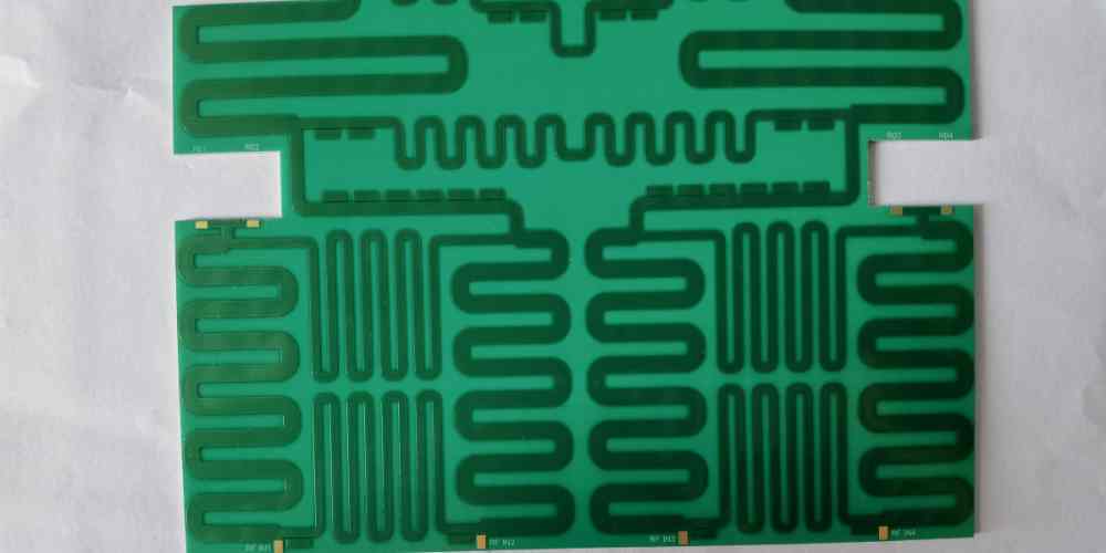
RF/microwave boards – Typically 0.25-0.38 mm since thinner material has lower loss at high frequencies. Thinner also reduces weight.
Power electronics – 0.38-0.64 mm provides good thermal performance while minimizing thickness. May go up to 1 mm for high voltage designs.
LED lighting – 0.25-0.38 mm gives good thermal conductivity for heat spreading while allowing thin luminaire profiles.
Automotive – 0.38-0.64 mm range meets mechanical strength and dielectric isolation needs in harsh environment.
Aerospace – As thin as possible (0.25-0.38 mm) ideal for weight sensitive applications with adequate dielectric strength.
Medical – 0.25-0.64 mm provides compact size while meeting electrical safety requirements.
Factors Influencing Alumina PCB Thickness
Thermal Performance
Thinner alumina PCBs provide lower thermal resistance for heat conduction from components to heat sinks. This improves cooling capabilities.
However, thinner boards are more prone to cracking from thermal stresses. So the thinness should be balanced with maintain reliability under thermal cycles expected in the application.
Dielectric Breakdown Voltage
Alumina PCB thickness must be sufficient to withstand expected operating voltages without electrical breakdown through the substrate. Minimum thickness is proportional to dielectric strength of the alumina and voltage levels.
Mechanical Strength
Thinner boards can warp or crack more easily under mechanical and thermal stresses. Minimum thicknesses are needed for handling during fabrication and assembly. Thicker boards provide higher strength at the expense of thermal conductivity and weight.
Substrate Material Loss
Thinner alumina PCBs have lower dielectric loss at RF/microwave frequencies for improved performance in high frequency circuits.
Component Height
For thick or multi-layer components like power semiconductors, thicker PCBs may be needed to contain the full component height. Recessed cavities can also provide clearance.
Manufacturing Constraints
Thinner PCBs can require more advanced machining and lamination processes. Cost factors may dictate thinner than ideal for highest performance designs.
Weight Considerations
Mass reduction is critical in aerospace, automotive and portable electronics applications. Thinner alumina PCBs help minimize weight while still providing excellent insulating properties compared to conventional PCB laminates.
Design Considerations for Thin Alumina PCBs
To leverage the benefits of thinner alumina PCBs, designers should account for the following:
- Warping stresses – Use symmetrically layered buildup, prevent extreme thermal gradients
- Cracking – Optimize board shape, hole placement and traces to avoid cracks
- Dielectric strength – Ensure sufficient insulating layers between conductors at potential voltages
- Stiffness – Ribbing, bonding stiffeners or special handling during assembly may be needed
- RF loss – Models may need to account for losses in thinner substrates
- Thermal vias – Help conduct heat from buried layers in thin boards
- Soldering – Adjust profiles to prevent overheating thin boards
Cross Section and Layer Structure
Alumina PCB cross sections can contain multiple layers built up on the alumina core substrate:
Alumina PCB cross section showing typical layer structure
Thin cores allow smaller vias and tighter routing while thick multilayer copper builds provide current carrying capability. Common arrangements include:
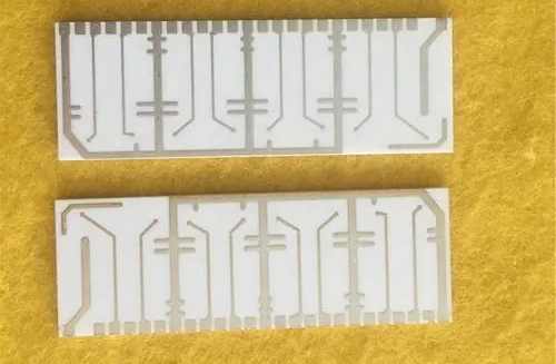
- Single sided – Traces on one side only for low complexity circuits
- Double sided – Traces on both sides with plated through holes (PTHs)
- Multilayer – Additional layers built up with buried and blind vias
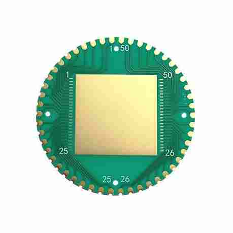
- Metal backing – Thin alumina on metal baseplate for thermal conduction
- Cavities – Metal layers etched away for mounting recessed components
The number of conductive layers can range from 1 to around 48 depending on design complexity. More layers allows higher circuit density.
Protective Coatings
Alumina PCBs utilize protective coatings to improve flexural strength, moisture resistance, dielectric isolation and electrical insulation:
- Conformal coating – Thin polymer layer enhances electrical insulation and protects against environmental contaminants. Often applied selectively over critical components and traces.
- Solder mask – Epoxy based coatings limit solder spreading and prevent bridging between pads during assembly. Withstands soldering temperatures. Photoimageable for patterned application.
- Gold plating – Thin immersion gold applied over nickel barrier improves solderability and wire bonding adhesion. Gold is biocompatible for medical devices.
Alumina PCB Thickness vs Copper Weight
Another consideration is matching alumina substrate thickness to the copper foil used for conductors. Standard foil thickness for traces and layers range from 0.5 oz (18 μm) to 6 oz (210 μm).
Guidelines for alumina thickness relative to copper weight:
| Copper Weight | Alumina Thickness |
|---|---|
| 0.5-2 oz | 0.25 mm |
| 1-4 oz | 0.38 mm |
| 2-6 oz | 0.64 mm |
Thicker copper foils are paired with thicker alumina cores which provide the stiffness required.
Thinner aluminum cores use thinner copper to help maintain mechanical integrity and reliability under bending and thermal stresses.
Alumina PCB Thickness vs Frequency
Electrical loss in the alumina substrate increases at higher frequencies. The chart below shows the trend of reduced loss for thinner alumina PCB substrates as frequency increases into the microwave region.
Dielectric loss tangents for 96% alumina PCBs of various thicknesses
This demonstrates why RF circuit and microwave PCBs utilize the thinnest alumina substrates possible, typically 0.25-0.38 mm.
Alumina PCB Thickness FAQ
How thick are alumina PCBs?
Alumina PCB substrate thickness typically ranges from 0.25 mm to 1.6 mm (0.010” to 0.063”). Most common is 0.25-0.64 mm (0.010” – 0.025”) for a balance of performance, manufacturability and durability. Thinner alumina provides better thermal conductivity and high frequency characteristics.
Why are alumina PCBs thin?
The high dielectric strength and thermal conductivity of alumina allows using thinner substrates than standard FR4 laminates. This improves thermal performance and reduces electrical losses. Thinner boards are also important for weight sensitive applications like aerospace, telecom and portable electronics.
What is the thinnest alumina PCB?
The thinnest readily available alumina PCBs are around 0.25 mm (0.010”) thickness. This is typically used for RF boards and microwave circuits where minimizing loss and weight are critical. 0.15 mm custom alumina PCBs have been demonstrated but are not in mainstream production.
What affects choice of alumina PCB thickness?
Key considerations for alumina PCB thickness include thermal conductivity, dielectric strength, mechanical rigidity, substrate losses at operating frequency, manufacturing constraints, component heights, and weight targets. The optimal thickness balances these electrical, mechanical, and physical requirements.
How thick should alumina PCB be for RF?
For RF circuits and microwave PCBs, thinner alumina substrates are desirable to reduce dielectric losses. 0.25-0.38 mm thick boards are commonly used to minimize signal loss at GHz frequencies while providing adequate structural strength for fabrication and assembly.


Leave a Reply