What is PCB Production?
PCB (Printed Circuit Board) production is the process of manufacturing electronic circuits by etching conductive pathways onto a non-conductive substrate. This process involves several steps, including designing the circuit layout, creating a photomask, applying photoresist, etching away unwanted copper, and finally, assembling components onto the board.
The Importance of PCB Production
PCBs are essential components in nearly all electronic devices we use today, from smartphones and computers to medical equipment and aerospace technology. The quality and reliability of these devices depend heavily on the precision and accuracy of the PCB production process.
The History of PCB Production
The concept of printed circuits dates back to the early 20th century when inventors began experimenting with printing conductive ink onto paper or cloth. However, it wasn’t until the 1940s that modern PCB production techniques were developed, primarily driven by the needs of the military during World War II.
In the 1950s, the introduction of photoresist and etching processes revolutionized PCB production, allowing for more complex designs and higher precision. The 1960s saw the advent of multi-layer PCBs, which further expanded the possibilities for circuit design.
The PCB Production Process
Step 1: Circuit Design
The first step in PCB production is designing the circuit layout using specialized software called EDA (Electronic Design Automation) tools. This involves creating a schematic diagram of the circuit and then translating it into a physical layout that specifies the location and interconnection of components on the board.
Step 2: Creating the Photomask
Once the circuit layout is finalized, a photomask is created. This is a transparent sheet with opaque areas that correspond to the desired conductive pathways on the PCB. The photomask is typically made using a high-resolution printer or a specialized photoplotter.
Step 3: Applying Photoresist
The next step is to apply a light-sensitive material called photoresist onto the copper-clad substrate. This can be done through various methods, such as dip coating, spin coating, or spray coating. The photoresist is then dried and cured to ensure proper adhesion to the substrate.
Step 4: Exposure and Development
The photomask is placed on top of the photoresist-coated substrate, and the assembly is exposed to ultraviolet (UV) light. The opaque areas of the photomask block the UV light, while the transparent areas allow it to pass through and react with the photoresist.
After exposure, the substrate is immersed in a developer solution that removes the photoresist from the areas that were exposed to UV light, leaving behind a pattern that matches the desired conductive pathways.
Step 5: Etching
The exposed copper areas on the substrate are then etched away using a chemical solution, typically ferric chloride or ammonium persulfate. This process removes the unwanted copper, leaving behind only the desired conductive pathways.
Step 6: Stripping and Finishing
After etching, the remaining photoresist is stripped away using a solvent or an alkaline solution. The PCB is then cleaned and inspected for any defects or irregularities.
Additional finishing steps may include applying a solder mask to protect the copper traces, adding silkscreen labels for component identification, and applying surface finishes such as HASL (Hot Air Solder Leveling) or ENIG (Electroless Nickel Immersion Gold) to improve solderability and protect against oxidation.
Step 7: Assembly and Testing
Finally, the electronic components are soldered onto the PCB using various techniques, such as through-hole mounting or surface-mount technology (SMT). The assembled PCB is then tested to ensure proper functionality and performance.

Types of PCBs
There are several types of PCBs, each with its own unique characteristics and applications. Some common types include:
| PCB Type | Description | Applications |
|---|---|---|
| Single-layer | Has conductive pathways on only one side of the substrate | Simple, low-cost devices |
| Double-layer | Has conductive pathways on both sides of the substrate | More complex devices, such as power supplies and amplifiers |
| Multi-layer | Has multiple layers of conductive pathways separated by insulating layers | High-density, complex devices, such as smartphones and computers |
| Flexible | Made from flexible materials, such as polyimide | Wearable electronics, medical devices, aerospace applications |
| Rigid-Flex | Combines rigid and flexible sections in a single PCB | Devices requiring both stability and flexibility, such as cameras and displays |

PCB Materials
The choice of materials used in PCB production can significantly impact the performance, reliability, and cost of the final product. Some common materials include:
Substrate Materials
| Material | Description | Applications |
|---|---|---|
| FR-4 | A composite material made from woven fiberglass and epoxy resin | Most common substrate material for general-purpose PCBs |
| Polyimide | A high-performance polymer with excellent thermal and chemical resistance | Flexible PCBs and high-temperature applications |
| PTFE | A fluoropolymer with low dielectric constant and high thermal stability | High-frequency and microwave applications |
| Alumina | A ceramic material with high thermal conductivity and dielectric strength | High-power and high-temperature applications |
Conductive Materials
| Material | Description | Applications |
|---|---|---|
| Copper | The most common conductive material used in PCBs | General-purpose PCBs |
| Gold | A highly conductive and corrosion-resistant material | High-reliability and high-frequency applications |
| Silver | A highly conductive material with excellent thermal conductivity | High-temperature and high-power applications |
| Aluminum | A lightweight and low-cost conductive material | Low-cost and high-volume applications |

PCB Manufacturing Methods
There are several methods used in PCB production, each with its own advantages and limitations. Some common methods include:
| Method | Description | Advantages | Limitations |
|---|---|---|---|
| Subtractive | Etches away unwanted copper from a fully copper-clad substrate | Simple and low-cost for low-volume production | Limited resolution and feature size |
| Additive | Deposits conductive material onto a non-conductive substrate | High resolution and fine feature size | Slower and more expensive than subtractive methods |
| Semi-additive | Combines subtractive and additive techniques | Balanced trade-off between resolution and cost | More complex process than fully subtractive or additive methods |
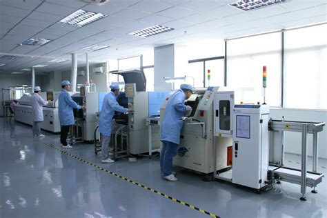
Quality Control in PCB Production
Ensuring the quality and reliability of PCBs is critical for the proper functioning of electronic devices. Some key aspects of quality control in PCB production include:
Visual Inspection
Visual inspection is the first line of defense against PCB defects. This involves examining the PCB for any obvious flaws, such as damaged traces, incorrect component placement, or solder bridging.
Automated Optical Inspection (AOI)
AOI systems use high-resolution cameras and image processing algorithms to detect and classify defects on the PCB surface. This method is faster and more consistent than manual visual inspection but may miss some types of defects.
X-ray Inspection
X-ray inspection is used to detect internal defects, such as voids in solder joints or misaligned components in multi-layer PCBs. This method is non-destructive and can provide detailed images of the internal structure of the PCB.
Electrical Testing
Electrical testing is performed to verify the proper functioning of the PCB and its components. This can include continuity testing, insulation resistance testing, and functional testing under various environmental conditions.
Future Trends in PCB Production
As electronic devices continue to evolve and become more complex, PCB production technologies must keep pace. Some future trends in PCB production include:
Miniaturization
The demand for smaller and more compact electronic devices is driving the need for higher-density PCBs with finer features and tighter tolerances.
3D Printing
Additive manufacturing techniques, such as 3D printing, are being explored as potential methods for creating complex, three-dimensional PCB structures with embedded components.
Sustainability
There is a growing emphasis on developing more environmentally friendly PCB production processes, such as using lead-free solders and reducing the use of hazardous chemicals.
Industry 4.0
The integration of advanced technologies, such as artificial intelligence, machine learning, and the Internet of Things (IoT), is expected to revolutionize PCB production by enabling smarter, more efficient, and more autonomous manufacturing processes.
Frequently Asked Questions (FAQ)
-
What is the difference between a PCB and a PCBA?
A PCB (Printed Circuit Board) is the bare board with conductive pathways etched onto it, while a PCBA (Printed Circuit Board Assembly) is a PCB with electronic components soldered onto it, ready for use in an electronic device. -
What is the typical turnaround time for PCB production?
The turnaround time for PCB production can vary depending on the complexity of the design, the chosen manufacturing method, and the volume of the order. Simple, low-volume PCBs can be produced in a matter of days, while complex, high-volume orders may take several weeks. -
What is the minimum feature size achievable in PCB production?
The minimum feature size depends on the manufacturing method and the capabilities of the specific PCB manufacturer. Modern PCB production techniques can achieve feature sizes as small as 50 microns (0.05 mm) or less. -
How do I choose the right PCB material for my application?
The choice of PCB material depends on several factors, such as the operating environment, the required electrical and thermal properties, and the cost constraints. Consult with your PCB manufacturer or a materials expert to select the most suitable material for your specific application. -
What are the environmental concerns associated with PCB production?
PCB production involves the use of hazardous chemicals and materials, such as lead, copper, and various solvents. Improper disposal of these substances can lead to environmental contamination and health risks. PCB manufacturers must adhere to strict environmental regulations and implement proper waste management practices to minimize these concerns.
Conclusion
PCB production is a complex and multi-faceted process that plays a crucial role in the development and manufacturing of electronic devices. Understanding the various steps, materials, and methods involved in PCB production is essential for designing reliable and high-performance electronic circuits.
As technology continues to advance, PCB production must adapt to meet the ever-increasing demands for smaller, faster, and more sophisticated electronic devices. By staying informed about the latest trends and developments in PCB production, engineers and manufacturers can ensure that they are well-positioned to meet these challenges and deliver cutting-edge electronic solutions.


Leave a Reply